advanced-packaging
(23)
KLA makes small mistakes a big business.
The chip industry keeps shrinking its circuits. KLA built a business around the errors that grow harder to see - and more expensive to miss.
Lam Research makes the cut
The chip industry dreams in three dimensions. Lam Research builds the machines that turn those dreams into working silicon, one carefully controlled layer at a time.
The chip is only the beginning.
Amkor turns silicon into something the world can use. Its expanding Arizona campus shows why the next contest in computing runs through packaging and test.
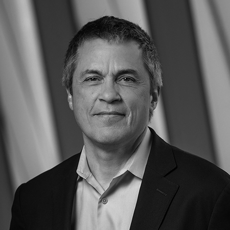
Rick Wallace and the case for taking the harder road
A hundred rejected applications sent Rick Wallace west in a Camaro. Four decades later, KLA’s CEO is still choosing the assignments that make him learn something new.
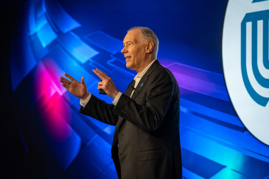
Gary Dickerson and the distance between an idea and a chip
After decades inside the machinery of chipmaking, Gary Dickerson is betting on a shorter route from discovery to production. His $5 billion EPIC Center puts that conviction under one roof.
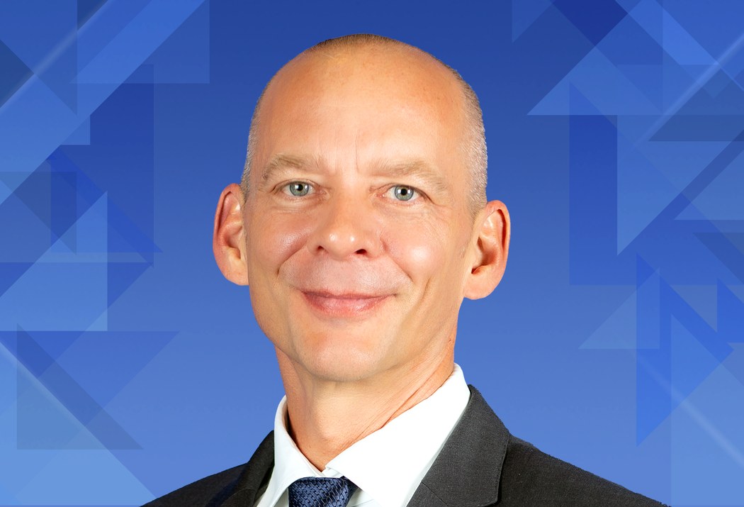
Kevin Engel and the importance of the last connection
He joined Amkor through an acquisition in 2004. Two decades later, the chemical engineer is leading the company as advanced packaging changes what a chip can do - and where it can be made.
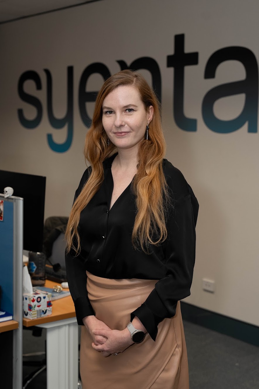
Jekaterina Viktorova and the trouble between the chips
A chemistry problem followed Jekaterina Viktorova from Germany to a Canberra lab and, for a while, her kitchen table. Now the Syenta co-founder is working on the tiny connections that help AI chips talk to each other.
The Billion-Dollar Bet on the Wires Between Chips
AI chips have become ravenous for data. Eliyan sells the connections that let compute, memory and whole packages keep up - and bets that cheaper packaging can be a competitive weapon.
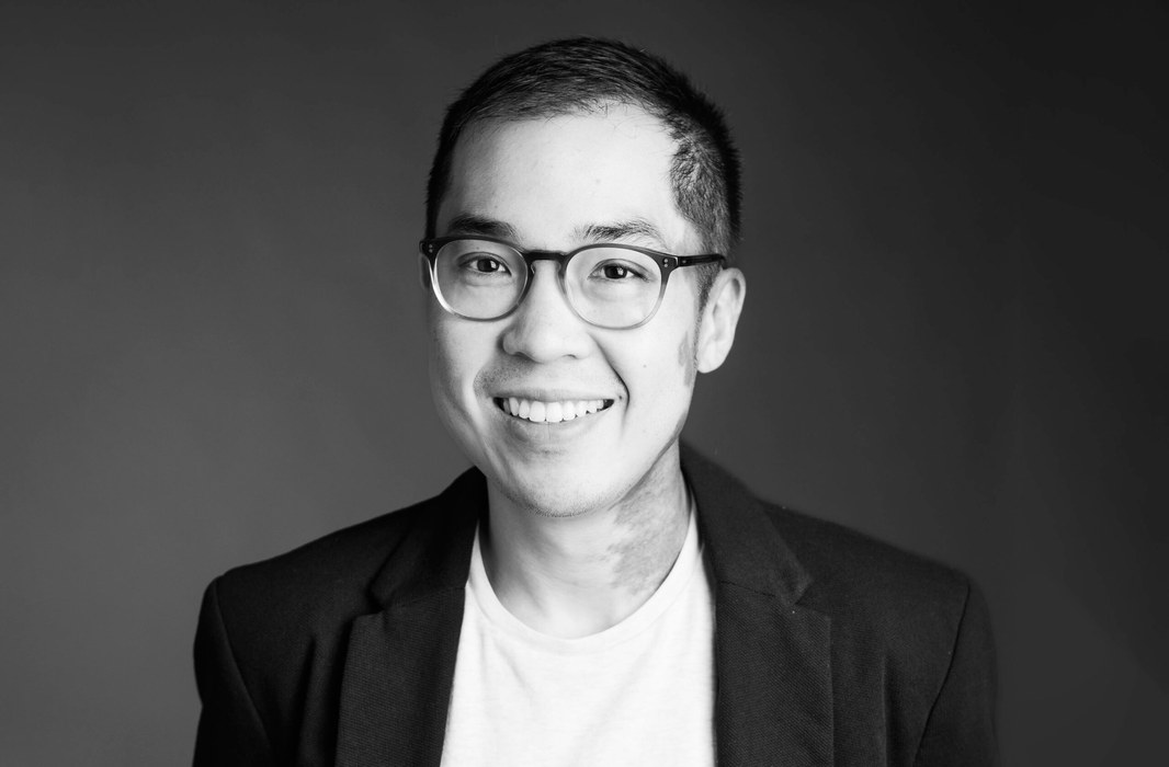
Darius Bunandar and the Art of Moving Light
He began with explosions, black holes and quantum-secure messages. Now Lightmatter's co-founder and chief scientist is trying to solve AI's less glamorous crisis: the costly distance between one chip and the next.
The Slow Beam Learned to Move in Parallel
Electron-beam lithography was always wonderfully precise and painfully slow. Multibeam's bet was that the beam did not need to become faster - it needed colleagues.
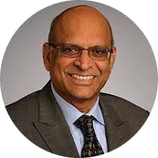
Babu Mandava Has Spent Four Decades Solving the Layer Beneath the Next One
From a first engineering post in India to WiMAX, LTE and glass-core packaging, Mandava's career follows a recurring question: what has to work underneath before the next computing market can scale?
The Machines That Teach AI Chips to Behave
Onto Innovation does not design the AI chip. It builds the eyes, rulers and feedback loops that help factories make those chips without wasting a fortune.

The Chip Giant That Quit the Nanometer Race - and Found Its Edge
GlobalFoundries walked away from the industry’s most expensive contest. Now its specialty chips sit inside phones, cars, factories and the optical plumbing of AI - a bet that useful can matter more than smallest.

Global Unichip Corporation (GUC)
The Taiwanese design house that quietly builds other people's AI chips - and reserved 60,000 CoWoS wafers to keep doing it.
SEMI
For 55 years SEMI has been the connective tissue of the chip industry - the neutral ground where rival equipment makers, materials suppliers and fabs agree on the rules, sizes and safety norms that let a wafer built in one country be tested in another.

Applied Materials
The company behind the machines that build almost every chip you own - and the atomic-scale materials engineering that keeps Moore's Law alive.
Teradyne
Most people never see a Teradyne machine, yet its testers stand between ambitious chip designs and the devices we trust. Now the 66-year-old Massachusetts company is applying the same factory-floor discipline to AI hardware, advanced packaging and robots that work beside people.
Stefan Pastine
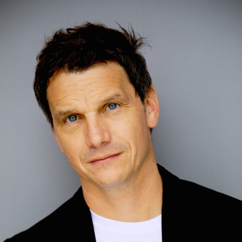
Stefan Pastine is an American chemist, inventor and deep-tech founder who builds materials most people never think about but every device depends on. After earning a PhD in organic chemistry from Columbia and doing postdoctoral work at UC Berkeley, he founded Connora Technologies to make recyclable epoxy resins, which was acquired by Aditya Birla Chemicals in 2019. That same year he founded Thintronics, a Bay Area startup developing next-generation dielectric insulator films for printed circuit boards and semiconductor packaging. His pitch is deceptively simple: the insulator, long ignored while engineers obsessed over transistors, is the overlooked bottleneck for faster, cooler AI data centers - and Thintronics wants to unseat a Japanese giant that has held 90% of the market for three decades.
Galatek
Galatek is a Singapore-based automation and AI company building intelligent infrastructure for two sectors where precision and data integrity matter most: life sciences and advanced semiconductor manufacturing. It pairs robotics and machine vision with software - its Abio platform unifying ELN, LIMS, SDMS and lab automation, and its InteVega AI vision platform - to run smart labs and inspect chips. Led by CEO David Tian, Galatek raised roughly US$30 million in a Series A round announced in December 2025 to expand across Europe, North America and Southeast Asia.

Syenta
Syenta is an Australian deep-tech semiconductor company building next-generation chip-to-chip interconnects for the AI era. Spun out of the Australian National University, it has developed a proprietary process called Localized Electrochemical Manufacturing (LEM) that deposits and patterns metal in a single step, producing micron-scale interconnects across large packages with fewer process steps. The technology targets the 'memory wall' that limits AI and high-performance computing, aiming to raise interconnect density and bandwidth while cutting manufacturing cost and waste. Headquartered in Sydney with a new development facility in Tempe, Arizona, Syenta has raised more than A$37 million, with former Intel CEO Pat Gelsinger joining its board.

3D Glass Solutions, Inc.
3D Glass Solutions (3DGS) is an Albuquerque, New Mexico advanced-packaging company that turns its patented photosensitive APEX glass-ceramic into precise 3D microstructures for chips. Its wafer-level glass substrates, interposers and integrated passive devices serve RF, photonics, high-performance computing and defense customers who need low-loss, high-frequency, thermally stable packaging. Spun out of technology developed at Sandia National Laboratories and led by semiconductor veteran Babu Mandava, the ISO 9001 / AS9100 certified foundry has raised more than $54 million, counts Intel Capital, Applied Ventures and Lockheed Martin Ventures among its backers, and is a partner in DARPA's Next-Generation Microelectronics Manufacturing (NGMM) program for U.S.-based 3D heterogeneous integration.

Ayar Labs
Ayar Labs is a San Jose-based semiconductor company building optical input/output (I/O) technology that moves data between chips using light instead of copper. Its silicon-photonics chiplets - the TeraPHY optical engine and the SuperNova multi-wavelength light source - are designed to be co-packaged directly with GPUs and other processors, letting AI and high-performance-computing systems scale across thousands of accelerators with far higher bandwidth and far lower power than electrical interconnects. Spun out of a DARPA-funded university research effort, the company raised a $500M Series E in 2026 with backing from NVIDIA and AMD.

Thintronics
Thintronics is a San Francisco-based advanced materials company reinventing the humble insulator - the dielectric films that sit between the copper layers of every chip and circuit board. Founded in 2019 by chemist Stefan Pastine, the company designs new insulating materials from the molecular level up, aiming to deliver faster, lower-loss, lower-power interconnects for AI data centers, high-speed networking, and RF/millimeter-wave systems. Its pitch is pointed: challenge the Japanese incumbent Ajinomoto, which has held more than 90% of the dielectric build-up film market for three decades, with a US-made alternative built for the terabit age.