Ken Levy had a manufacturing problem. His company made machines that helped semiconductor manufacturers find mistakes, but getting those machines out of its own factory on time and on budget was proving difficult. He began buying lunch for an operations specialist, Ken Schroeder, and asking for advice. After several lunches, Levy offered him a job. The man helping to fix the factory would eventually run the company.
- KLA helps chipmakers find defects and measure whether production is staying on target.
- Its customers buy better yield: more working devices from their manufacturing effort.
- Equipment sales lead to years of maintenance, support and upgrades.
The factory needed a factory man
The anecdote, which Levy told in a 2004 oral history, is a useful entrance to KLA. Expertise was valuable, but it had to reach a working production line. Levy and Bob Anderson started with $600,000 from EG&G and Continental Capital. Making the technology reliable enough for production took time. Having an idea customers wanted was only the beginning.
There had also been a question of focus. In a Stanford talk, Rick Wallace recounted an early plan that included both mask inspection and blood analyzers. Investors insisted the startup choose. It chose masks: the patterned templates used to transfer circuit designs. The two businesses shared image-processing ideas. They did not share the same customer problem. That distinction mattered.
“You need to focus.”
Rick Wallace, recounting early investor advice at Stanford, 2006
The profit hiding in the rejects
Chipmaking has a peculiar arithmetic. A factory can complete an enormous amount of technically impressive work and still produce devices it cannot sell. Yield measures how much of that effort becomes functioning product. An error discovered late has already consumed more materials, equipment time and processing. An error discovered early gives an engineer a chance to stop repeating it.
KLA supplies the looking and measuring. Its inspection systems locate defects; its metrology systems measure dimensions, film thickness and the alignment of layers. Its buyers include foundries, memory manufacturers, wafer and reticle suppliers, and packaging companies. The practical question for these customers is whether a process is drifting before the drift becomes a shipment problem.
Same wafer. More working chips.
Imagine 100 potential chips. Change the yield to see how many become usable.
The product names sound like equipment from a science-fiction loading dock: Archer, Axion, Voyager. Their jobs are quite specific. Archer measures whether patterned layers line up. Axion uses X-rays to measure three-dimensional memory structures without cutting them apart. The 3935 inspector uses broadband plasma illumination to find defects on advanced wafers. These are different ways of answering a factory’s questions.
A sensitive detector alone is insufficient. The system has to distinguish consequential defects from noise and move fast enough for production. KLA’s software, including Klarity, helps analyze the resulting data. The useful output is information an engineer can act on: where a problem occurred, what it resembles and whether the process needs attention.
For a process engineer, this changes the order of the investigation. A disappointing final result tells you something went wrong. Measurements between production steps help narrow down when it happened. That is why inspection belongs inside the manufacturing process, with results feeding back into the next decision. Waiting until the end throws away opportunities to intervene.
The sale that keeps working
In fiscal 2026, KLA reported $13.58 billion in revenue. About $3.13 billion came from service. An installed inspection machine needs support, maintenance and, over time, improvements. That continuing relationship gives KLA a business beyond the initial equipment purchase, while giving the customer a reason to care about the supplier’s staying power.
The commitment runs both ways. KLA spent approximately $1.53 billion on research and development that year. Its customers’ next manufacturing problems cannot wait for the current tools to become obsolete. Physics, optics, sensors and algorithms have to advance together. In Ann Arbor, its AI and Modeling Center of Excellence brings software, machine-learning and hardware engineers into that work.
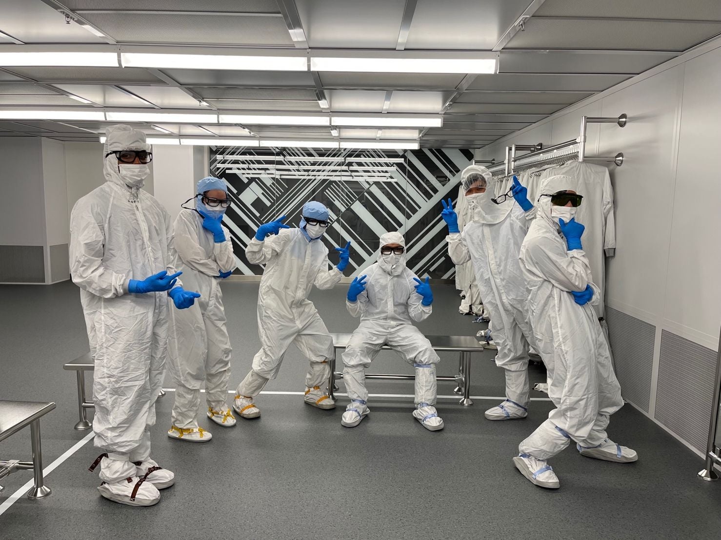
KLA describes its culture through perseverance, improvement, teamwork, honesty and being indispensable to customers. The last ambition has a practical test: does the equipment keep helping when the customer changes materials or processes? A supplier earns that relationship through application knowledge as well as hardware. The work continues after an instrument is installed.
Too useful to lock away
There is a revealing episode in KLA’s competitive history. In 2016, it and Lam Research abandoned their proposed merger after antitrust concerns. The US Justice Department worried that a combined company could restrict Lam’s competitors’ timely access to KLA’s inspection and metrology equipment. Tools used to understand a process could influence who got to improve that process.
That helps explain KLA’s position among equipment suppliers. It competes with Applied Materials, ASML, Hitachi High-Tech, Lasertec and Onto Innovation in different parts of its portfolio. Its proposition rests on combining measurement expertise, analysis and service across manufacturing steps. A customer still has to evaluate the particular application. No single supplier’s catalogue makes every instrument interchangeable.
The mistakes move into the package
KLA has widened the territory it serves. Its 2019 acquisition of Orbotech carried approximately $3.26 billion in purchase consideration, extending its reach into printed circuit boards, displays, packaging and related manufacturing. Expansion has required choices, too: KLA subsequently exited the display business. Buying a broader portfolio did not make every market a permanent commitment.
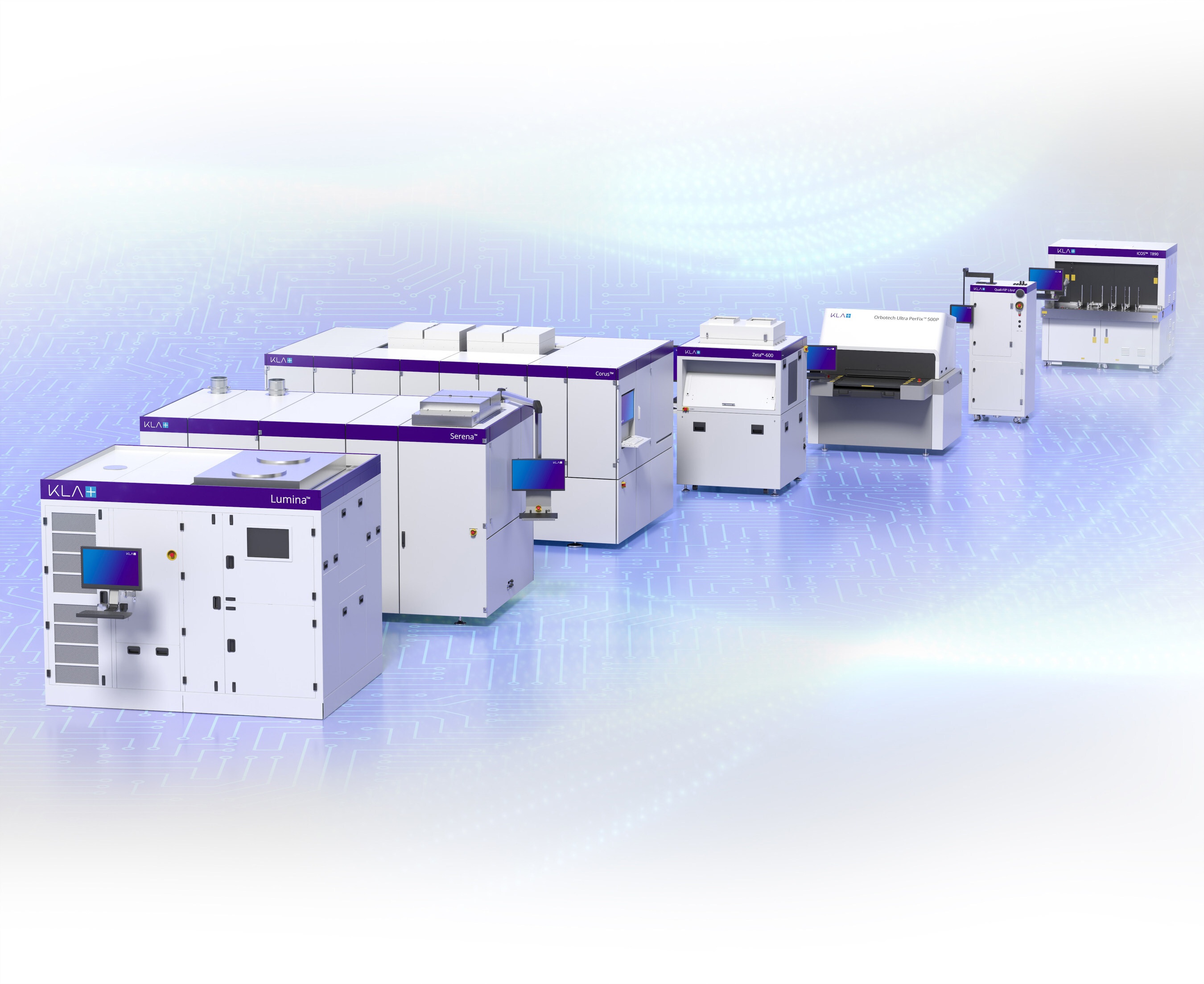
The 2024 substrate portfolio shows where its expertise travels next. Serena and Corus handle direct imaging; Lumina provides inspection and metrology for advanced substrates and panel-based interposers, including glass-core applications. As packages connect multiple components, the connections themselves become manufacturing challenges. The inspection problem follows the complexity beyond the wafer.
Research partnerships extend the same logic upstream. KLA and imec announced an intended automotive talent and research initiative in 2023; KLA also joined imec’s 300mm gallium nitride program as an early partner in 2025. Understanding tomorrow’s materials gives an equipment maker a chance to prepare its measurements before customers need them in volume production.
Measure where a decision can change
KLA’s transferable lesson is to find an expensive, recurring failure and measure it early enough to change the outcome. There is a boundary to that advice. Inspection must justify its cost, speed and operational burden. On a simpler process, a cheaper instrument may suffice. A measurement nobody can use becomes another expense. Its usefulness depends on that timing.
The next test is already on the calendar: KLA’s September-quarter results are scheduled for October 28, 2026. But the underlying question has survived generations of chips. How much would you pay to discover a mistake while you can still do something about it?