In the late 1970s, David Lam saw a problem that had little to do with imagining a smaller chip. Engineers already knew about plasma etching, the technique of using energized gases to remove material. What troubled him was the equipment. A promising process still needed a machine a factory manager could depend on. The distance between those two things would become a company.
- Lam sells the tools that add, carve, and clean the layers of a chip.
- Its buyers include TSMC, Samsung, Micron, and SK hynix.
- More complicated chips create more demanding manufacturing work.
One wafer was the point
Lam founded his namesake business in 1980. Its first product, AutoEtch, arrived in 1981. In his oral history, he was careful about the invention story: plasma etching had existed for years. His opportunity was making it practical. Processing wafers individually offered a way to control the conditions around each wafer, rather than treating a batch as the basic unit.
This is a useful correction to the familiar Silicon Valley origin tale. The opening was a production problem that customers could recognize. A technique published in a paper and a technique trusted on a factory floor are different commercial propositions. Lam built around the second. The business went public in 1984.
The factory behind the factory
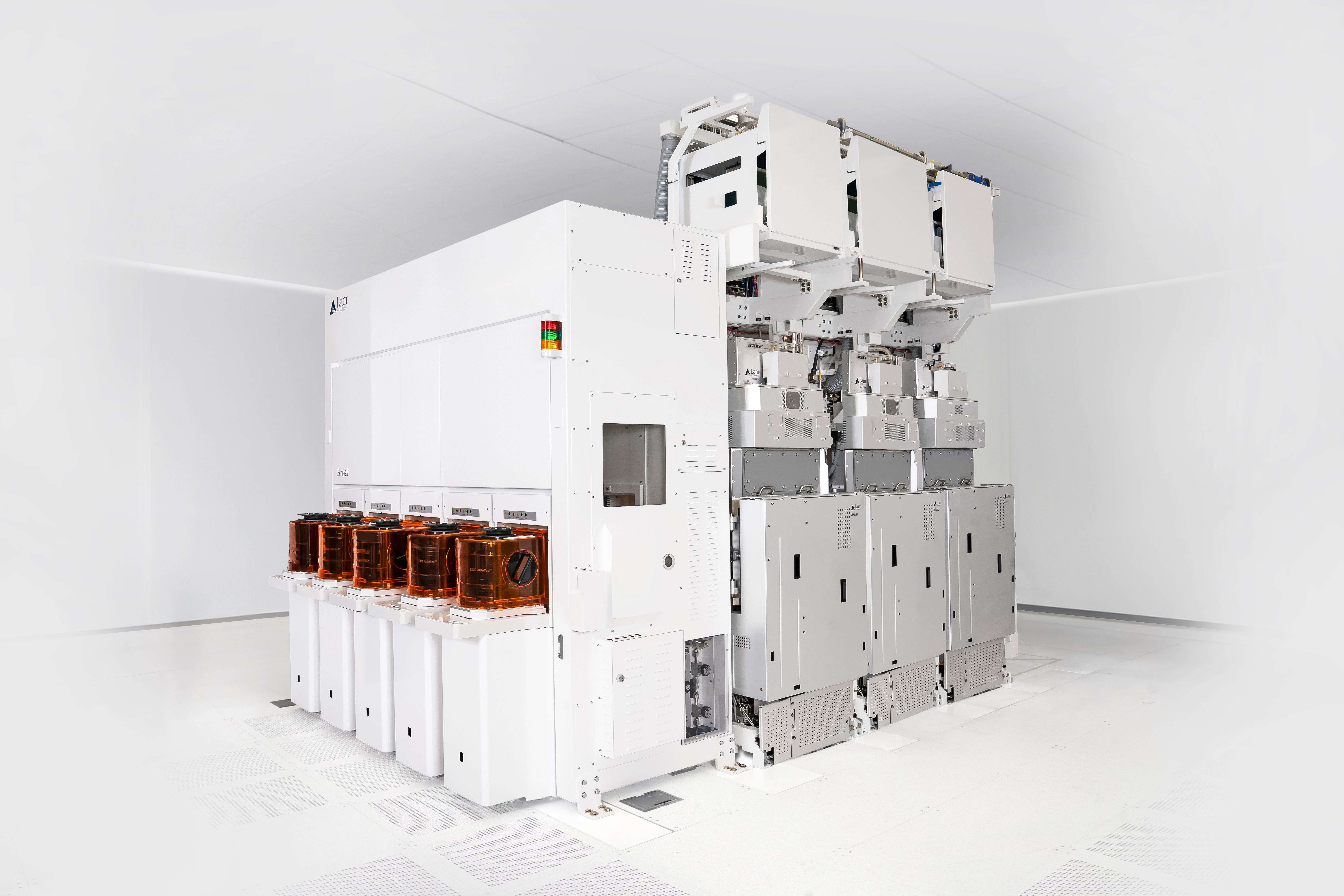
Today, Lam occupies a specific part of the semiconductor supply chain. Chip designers specify what circuits should do. Manufacturers build them. Lam supplies equipment for several of the physical operations in between: depositing films, etching selected material away, and stripping or cleaning what remains. Its expertise combines plasma physics, chemistry, materials science, and systems engineering.
The buyer is a fab, the factory where chips are made. Foundries manufacture for other companies; memory makers produce devices such as DRAM and NAND. Lam’s major customers include TSMC, Samsung, Micron, and SK hynix. These are technically demanding organizations buying production capability. A tool has to fit a process flow, work with neighboring steps, and make enough usable output to justify its place.
Competitors vary with the task. Applied Materials and Tokyo Electron compete in etch; ASM International competes in deposition categories; SCREEN competes in wet cleaning. ASML’s lithography systems perform a complementary job, exposing patterns. Lam’s proposition depends on how well it creates the material structures around those patterns. A chip factory needs several kinds of specialist.
A machine with a long afterlife
There is a practical distinction here for anyone trying to understand what they could do with Lam’s products. A fab engineer can use them to build and refine manufacturing steps; a chip designer depends on the manufacturing capabilities those steps make possible. Someone developing an AI application encounters the result further downstream, inside the processors and memory they use. The connection is indirect but consequential. A clever circuit delivers little value if it cannot be manufactured reliably. The equipment supplier’s contribution is to turn a difficult physical operation into something a customer can repeat, inspect, maintain, and eventually improve across a production line.
Equipment delivery begins another relationship. Tools need spare parts, maintenance, and upgrades. Lam sells those too. Its customer support-related revenue category also includes new and refurbished equipment for less advanced manufacturing through Reliant. Treating that entire category as a subscription would misread the business. It contains hardware as well as support.
The scale is considerable. For the quarter ended September 27, 2026, Lam reported $8.22 billion in revenue: roughly $5.73 billion from systems and $2.49 billion from customer support-related revenue and other. That second stream represented about 30% of the total. An installed machine creates years of engineering work, and an opportunity to keep helping the customer produce.
A bigger toolbox, with limits
Lam expanded its range by completing the Novellus merger in 2012, bringing additional thin-film deposition capabilities alongside etch and cleaning. The industrial logic is straightforward: adding a layer and removing parts of it are connected problems. Understanding both can help engineers solve the overall manufacturing task.
Another proposed combination stopped. In October 2016, Lam and inspection-equipment supplier KLA-Tencor abandoned their merger after antitrust feedback. Japan’s competition regulator had raised concerns about competitors’ access to KLA’s equipment and services. The companies reconsidered because the regulatory path had changed. Neither owed a termination fee. The episode exposed a boundary: combining complementary businesses can also unsettle the market around them.
Demand supplies another boundary. Lam’s fiscal 2024 revenue fell to $14.91 billion from $17.43 billion a year earlier, mainly because customers reduced nonvolatile-memory spending. Even sophisticated equipment depends on customers wanting more capacity or a new process. Technical progress does not abolish the spending cycle.
The next constraint is a material
As chips become more three-dimensional, making them involves awkward shapes and increasingly unforgiving tolerances. Akara, introduced in 2025, addresses conductor etch. Lam says its DirectDrive solid-state plasma source responds to process changes more than 100 times faster than previous sources. The claim concerns plasma responsiveness, rather than a hundredfold increase in finished chips.
ALTUS Halo, launched alongside Akara, tackles a different constraint: electrical resistance in shrinking metal features. It deposits molybdenum using atomic layer deposition. Aether, Lam’s dry resist technology, works around EUV patterning. These products address different points where a design can become difficult or expensive to manufacture.
“Drive semiconductor breakthroughs that define the next generation.”Lam Research’s stated mission
For the buyer, the purchase decision extends beyond the machine’s invoice. A process that produces fewer defective wafers can change the economics of an entire line. So can a tool that spends less time waiting for maintenance. The sensible comparison is the cost of useful output over time. This helps explain why close customer engineering matters: a result achieved on a demonstration wafer still has to survive the customer’s materials, recipes, production targets, and maintenance schedule.
That ambition carries a substantial bill. Fiscal 2026 research and development spending was about $2.38 billion. Collaboration spreads the technical work: Lam developed dry resist with ASML and imec, and announced a five-year IBM agreement in March 2026 aimed at processes for future sub-1nm logic nodes. That is a research destination, not a promise of a production date.
For anyone building a business, the transferable lesson is wonderfully concrete: find the step that prevents a customer from getting a reliable result. Then measure whether fixing it pays. Lam’s tools make sense where better yield, control, or uptime warrants the investment. Where an existing process already does the job economically, novelty alone offers a weak reason to replace it.