The short version
- Multibeam writes chip patterns directly with several miniature electron-beam columns operating at once.
- The pitch is not “replace every optical tool.” It is “skip the mask where flexibility is worth more.”
- Its named customers are SkyWater Technology and Taiwan's National Tsing Hua University.
- The repeatable lesson: take a beloved capability, find its fatal bottleneck, then divide that bottleneck into parallel work.
In a semiconductor factory, waiting can be astonishingly expensive. A chip designer changes a line. The new line needs a new optical mask. The mask is an immaculate stencil, engineered to project a pattern onto silicon, and it may take weeks to arrive. During those weeks the idea remains an idea. This is perfectly sensible when a factory intends to print the same thing millions of times. It is less charming when the whole point is to discover which thing should be printed.
Electron-beam lithography offered the obvious escape. It could draw straight onto the coated wafer from a digital design, like an impossibly fine pencil. No mask. Beautiful resolution. Curves, radial lines, one-off identifiers, last-minute changes - all fair game. It also had the productivity of an impossibly fine pencil. One beam writing a large wafer is still one beam writing a large wafer.
That was the first failure, and it arrived before Multibeam had a product: precision alone was not a market. When David K. Lam took charge around 2010, the grand notion that multi-beam systems might broadly displace optical lithography had run into a risk-averse industry and a throughput problem. Lam knew the industry from the machinery outward. He had founded Lam Research, built a market for automated single-wafer plasma etching and taken that company public. His second lithography act began with a retreat from the universal answer.
The useful question was no longer, “Can electrons replace light?” It was, “Where is waiting for a mask the expensive part?”Multibeam's strategic turn, in one sentence
Four pencils, one wafer
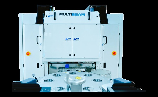
Multibeam's answer is architectural. It shrinks the electron columns, places several in an array and lets them operate independently and in parallel. An orchestration layer sends each beam to its piece of the pattern. Automated wafer loading, alignment, calibration and vacuum recovery do the less glamorous work required of a real fab tool. Synopsys CATS software converts familiar GDSII and OASIS design files into write recipes. A clever physics demonstration becomes a workflow that an actual process team can use.
One exquisite writer creates a queue. Several coordinated writers create throughput.
The company says the MB platform is more than 100 times as productive as conventional e-beam systems. It offers 150, 200 and 300 millimeter wafer configurations and can add writing modules. Those are vendor claims, but the commercial milestones are concrete. In June 2024, SkyWater Technology ordered the first system for early prototypes and rapid production of high-mix chips and microdevices. That mattered because a machine sold into a foundry has crossed a border that a laboratory prototype has not.
The odd jobs became the right jobs
What changed Multibeam's mind was not one discovery. It was a cluster of awkward manufacturing jobs. Advanced packaging needs tiny connections between chiplets that may not land in precisely the intended spot. Photonics needs gratings and waveguides with fussy geometries. Compound semiconductors and MEMS introduce topography that a shallow-focus process dislikes. Prototype teams want a hundred variations now, not one frozen design after the mask shop calls back.
Direct write has a peculiar advantage in these cases: it can respond to the object in front of it. Measure where a die actually landed, then adapt the connection pattern. Draw a curve as a curve. Put several experiments on one wafer. Give each chip a distinct security mark. The system is not merely maskless; it is allowed to be indecisive until late in the process. In manufacturing, indecision is usually a defect. During learning, it is an asset.
The pattern is settled, the volumes are enormous and the cost of a mask can be spread across many identical wafers.
Patterns change often, every die may differ, surfaces are awkward or waiting weeks for a mask costs more than writing time.
This is also the answer to the competitive question. Multibeam sits beside optical scanners, laser direct-write tools and conventional single-column e-beam machines. It does not need to beat optical lithography at the optical lithography game. It needs to win the layers where fixed masks and repeatable grids become liabilities. A commodity logic layer made by the million is a poor showcase. A quick-turn photonic device or an interposer whose lines must meet chiplets where they actually sit is a much friendlier one.
A machine company crosses the ocean
Deep hardware companies do not scale by uploading a signup form. They need application engineers, installation crews, customer trust and a service response measured against factory downtime. Multibeam chose partners accordingly. Synopsys supplies the data-preparation bridge. Marketech International supplies local reach and systems experience in Taiwan. BEAMS, part of the Marubeni Group, supports Japan.
The Taiwan sequence is particularly tidy. Multibeam named Marketech its regional partner in October 2025. In July 2026, National Tsing Hua University's College of Semiconductor Research ordered the new MBX platform after an evaluation, with delivery planned for 2027. The university intends to use it for academic work and joint development projects with Taiwanese chipmakers. It is a customer, a training ground and a window into the densest semiconductor neighborhood on earth.

Capital followed the customer evidence. A July 2025 Series B began at $31 million, led by Onto Innovation and Lam Capital, with UMC Capital and MediaTek Capital participating. By August 2026, Multibeam said the round had grown to $50 million and that it had added $15 million in venture debt. Separately, it signed a letter of intent with the U.S. Department of Commerce for up to $140 million in proposed funding for advanced-integration research. “Up to” and “proposed” do important work there. The company has also moved into a larger Silicon Valley headquarters with more manufacturing and R&D capacity.
The copyable part is not the electron
Most readers cannot build an ultra-high-vacuum lithography tool before lunch. The reusable move is simpler. Find a capability everyone admires but nobody deploys because of one ruinous constraint. Do not sand down the admired part. Reorganize the constraint. Multibeam kept the precision and split the writing work. Then it stopped chasing the entire fab and found customers for whom flexibility had a cash value.
Preserve the magic. Parallelize the bottleneck. Integrate the boring software. Enter through the job where delay is already expensive.
There are conditions attached. Parallel writers still do not make masks irrational for stable, enormous production runs. New capital equipment must survive uptime, yield and service demands that a slide deck never encounters. Adaptive writing matters only when the process can measure, prepare and feed the right data quickly. And customers must value time-to-learning enough to change a qualified flow.
That is why SkyWater and NTHU matter more than adjectives. They turn Multibeam's claim into two testable settings: a production foundry and a research institution connected to industry. The company has not made the mask disappear from semiconductor manufacturing. It has made the mask optional in a set of places where “optional” can save weeks. Sometimes a technology enters the mainstream by becoming universal. Sometimes it gets there by finally admitting what it is for.