semiconductor-manufacturing
(10)
The Slow Beam Learned to Move in Parallel
Electron-beam lithography was always wonderfully precise and painfully slow. Multibeam's bet was that the beam did not need to become faster - it needed colleagues.
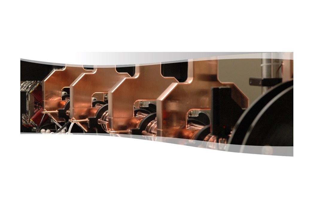
The Synchrotron That Fit in a Room - Until the Bet Got Bigger
Lyncean proved a national-lab machine could become a laboratory appliance. Then a far larger gamma-ray contract exposed the unforgiving economics of frontier hardware.
Noah Vogel Wants to Shrink the Cleanroom Until It Fits Around a Wafer
A freshman NASA proposal became a reactor, then a company, then a wager on the geometry of chipmaking: clean the few cubic feet around the wafer instead of an entire factory.

Mark Granahan Retired. Then He Found a Better Way to Use Silicon.
A retired chip executive went back to the journals, rented time in a university nanofab, and spent seven years proving that ordinary silicon still had another act.
Andrei Iancu Is Teaching Factories to Cut Crystals With Light
The Halo Industries founder turned a Stanford materials problem into a semiconductor manufacturing company. His wager is practical: waste less of the crystal, learn faster on the factory floor, and let better power electronics follow.

EthonAI
EthonAI (now branded Ethon) is a Zurich-based industrial AI company, spun out of ETH Zurich in 2021, that builds a Manufacturing Analytics System for factories. Its no-code platform layers on top of existing factory data sources to detect visual defects, monitor processes and run autonomous root cause analysis, using causal AI to explain what drives production variation. Customers including Siemens, Lindt & Sprüngli, Bosch and Roche use it to cut quality losses by up to 50% and raise productivity while keeping engineers in the decision loop.
Halo Industries, Inc.
Halo Industries is a Santa Clara deep-tech company that uses lasers instead of diamond wire saws to slice silicon carbide crystal boules into wafers, the foundational substrate for high-voltage power electronics. Spun out of Stanford in 2014, its proprietary light-based process aims to eliminate kerf loss, cut defects, and slash water and energy use, giving more usable wafers from every expensive crystal. Backed by an $80M Series B, Halo is scaling SiC production for electric vehicles, grid infrastructure, renewables, and aerospace, and extending the same approach to silicon, sapphire, and diamond.
Averroes.ai
Averroes.ai is a San Mateo-based startup building a no-code AI visual inspection platform that helps manufacturers automatically detect, classify, segment and monitor defects on their production lines. Founded in 2021 by Tareq Aljaber and Omar Altamimi, the company targets semiconductor, electronics, pharmaceutical, food and beverage, and oil and gas producers, promising 99%+ inspection accuracy, deployment in under five days, and models trained on as few as 20-40 images per defect class without writing code or buying new hardware.

Arno Merkle
Arno Merkle is the co-founder and CEO of Crystal Sonic, a Phoenix deep tech startup whose patented Sonic Lift-Off technology uses sound waves as an 'acoustic scalpel' to split thin device layers off semiconductor wafers so the costly substrate can be reused. A materials scientist with a Ph.D. from Northwestern and more than 75 technical papers to his name, Merkle spent two decades building and exiting X-ray and electron microscopy companies (Xradia, acquired by Carl Zeiss in 2013; XRE, acquired by Tescan in 2018) before turning his attention to one of chipmaking's quietest scandals: that conventional wafering throws away 90% or more of pristine, expensive crystal. With Crystal Sonic he is trying to make next-generation chips cheaper and far less wasteful, one sound wave at a time.
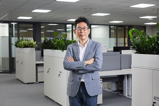
Mike Young-Han Kim
Mike Young-Han Kim is the founding CEO of Gauss Labs, a Palo Alto-based industrial AI startup revolutionizing semiconductor manufacturing. An 11th-generation academic descendant of Carl Friedrich Gauss, he holds a PhD in Electrical Engineering from Stanford along with dual master's degrees in EE and Statistics. Before founding Gauss Labs in 2020, he was a tenured IEEE Fellow professor at UC San Diego and the inaugural recipient of the James L. Massey Research & Teaching Award. Backed by $55M from SK hynix, his company's Panoptes VM platform now inspects over 50 million wafers at SK hynix facilities - at one wafer per second - reducing process variability by 29%.