Here is a fact that sounds like it can't possibly be load-bearing but is: to make a silicon carbide wafer, you take a cylindrical crystal that cost a great deal of money and time to grow, and you saw it into slices with a wire coated in diamond, because silicon carbide is so hard that ordinary blades give up. And every pass of that saw turns a slab of the crystal - the width of the cut, called the kerf - into powder. You paid for that powder. It is now dust.
Nobody loves this. It's just how it was done, the way it had always been done, and in most materials the loss is annoying rather than ruinous. Silicon carbide is not most materials. It is one of the hardest things made at industrial scale, it is expensive, and demand for it is climbing because it is the substrate underneath the power electronics in electric vehicles, EV chargers, solar inverters, wind turbines, and the electrical grid. So a company that could stop making dust would, in a fairly direct way, be making the electrification of everything a little cheaper.
The pitch is almost suspiciously simple: stop making dust. The engineering to deliver it took about ten years.
That company is Halo Industries. It was spun out of Stanford in 2014 - the founding idea came from PhD research on ultra-thin manufacturing methods for next-generation wafers, originally aimed at solar. The three co-founders are Andrei Iancu, who is CEO and whose academic training spans electrical, aerospace, and mechanical engineering; Philip Van Stockum, the CTO; and Charlie Rudy. Over time the company pointed its technology at the material the market actually wanted badly, which was silicon carbide.
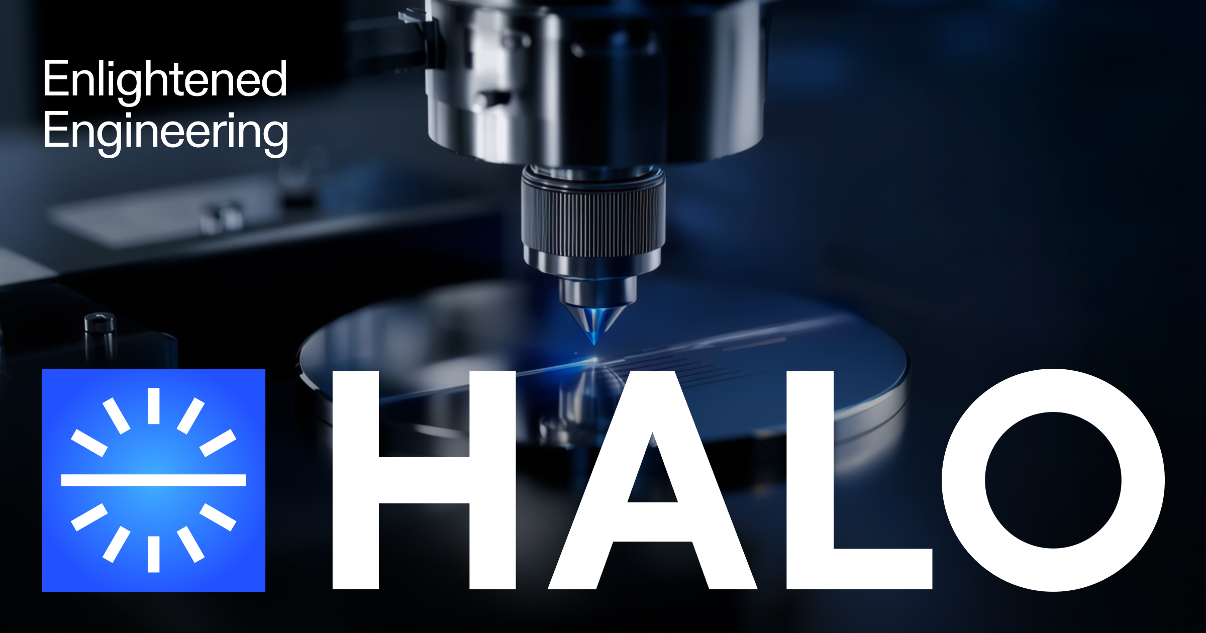
Halo's answer to the kerf problem is to replace the mechanical and thermal steps of wafering with light-based ones. Instead of dragging a diamond wire through the crystal, its proprietary multi-step laser process separates wafers with a beam. There is no blade width to lose, which means more usable wafers come off each boule. The company also says the approach reduces defects like wafer bow - the subtle warping that can render a slice useless - and cuts the water and energy that conventional wafering guzzles. The brand line for all of this is "Enlightened Engineering," which is either a pun you'll forgive or one you won't, but it is at least literally true.
The economic logic here is the interesting part. You could try to win in semiconductors the usual way, by building enormous fabs and racing costs down through scale and cheap labor. Halo's bet, and its investors' bet, is different: win on the physics of a single step so thoroughly that the math changes for everyone downstream. As the lead investor put it, the idea is that U.S. companies can onshore manufacturing "by competing on innovation, efficiency and cost" rather than by out-cheaping the world. That's a more appealing story if you believe it, and in July 2024 a lot of money decided to.
Specifically, Halo closed an oversubscribed Series B of up to $80 million, led by Thomas Tull's U.S. Innovative Technology Fund, with participation from 8VC and the engineering firm SAIC. Reports put the company's value near $300 million afterward. CEO Iancu framed the raise the way founders do - as "the foundation for our future strategic engagements where our innovations can reshape market economics" - which is a lot of syllables for "now we build the factory."
And building the factory is the actual hard part, which is worth being honest about. A laser that slices one wafer beautifully in a lab is a science result. A room full of those lasers that runs every shift, hits yield targets, and turns out tens of thousands of wafers a month is a manufacturing company, and the distance between the two has swallowed many good ideas. Halo's stated ramp - from roughly 1,000 wafers a month toward 24,000 - is a plain statement of exactly that gap and its intention to cross it. A California Energy Commission project, published in 2024, backed up the underlying claim, demonstrating laser SiC wafering with near-zero material loss.
A laser that slices one wafer is a science result. A room full of them running every shift is a company.
The most recent tell that Halo is getting serious about the boring, essential middle of that journey came in March 2026, when it picked Eyelit Technologies' AI-powered manufacturing execution system to run and scale its wafering line. That is not a headline-grabbing announcement. It is, however, exactly the kind of decision a company makes when it has stopped proving the concept and started running a production floor - choosing the software that tracks recipes, flows, and process data across a growing fleet of tools. Halo's production manager cited features for dynamic recipe configuration and for shielding proprietary process data, which tells you the company thinks its secret sauce lives in the details of how it runs the process, not just in the laser itself.
What can you actually do with Halo, if you're not Halo? If you make power electronics, the promise is more usable, higher-quality SiC wafers per crystal, at lower cost and with a smaller environmental footprint - the raw material for the chips that sit in inverters and chargers you'll never see. And because the same laser trick works on other stubborn materials - the company has demonstrated silicon, sapphire, diamond, gallium nitride, and lithium tantalate - the addressable problem is broader than any single wafer. It's the general problem of cutting hard, valuable crystals without wasting them.
The competition is real: incumbents like Wolfspeed, Coherent, onsemi, and SK Siltron, plus rival advanced-slicing methods such as Infineon's cold-split and DISCO's laser process. Halo is not alone in noticing that the saw is the problem. It is, at least, one of the companies that took a decade to do something specific about it - and then went and raised the money to find out whether the factory can keep up with the physics.