Before Tim Archer was responsible for the equipment behind other people’s chips, he was a Caltech student discovering the pleasure of making something himself. The class he remembers was Applied Physics 9 Lab. Theory became an object. An idea acquired edges. Decades later, the president and CEO of Lam Research still described the appeal in pleasingly ordinary terms: “you got to make something, hold it in your hand, and see real results.”
There are grander origin stories available to a technology executive. Archer’s has the advantage of being useful. A laboratory gave him a direction; his career took him through process development, equipment businesses, sales and operations. In 2025, he and Sandra Archer supported a new nanotechnology teaching laboratory at his old university. Somewhere inside the business of making very small things, a student’s practical education had become a personal investment.
A career with its sleeves rolled up
Archer graduated from Caltech in 1989 with a bachelor’s degree in applied physics. That year he began at Tektronix, developing processes for high-speed bipolar integrated circuits. His first professional work concerned how chips were actually made. The word “process” can make an occupation sound bloodless. Here it means persuading materials, equipment and a sequence of operations to produce the intended electronic device.
He joined Novellus Systems in 1994. Over an 18-year stretch, he moved through technical and business responsibilities, including a posting as senior director of technology for Novellus Systems Japan from 1999 to 2001. He later led the company’s PECVD and Electrofill businesses. The first involves depositing thin films; the second helps create metal connections. Both put him close to the unglamorous particulars on which a glamorous finished product depends.
A January 2006 announcement offers a small, concrete marker along that route. TSMC recognized Novellus’s SABRE NExT copper Electrofill system with a 2005 Best Product Award. Archer, then a senior vice president responsible for the Electrofill business, spoke about the customer’s manufacturing requirements. The achievement belonged to a tool and the people behind it. It is a useful glimpse of his working world: success measured in somebody else’s factory.

The customer’s factory is the examination room
By 2009, Archer’s remit included worldwide sales, marketing and customer satisfaction. In January 2011 he became Novellus’s chief operating officer. The progression matters because it crossed the gap between inventing equipment and keeping a business accountable for it. A technical proposition eventually has to survive a purchasing decision, installation and repeated use. Customers tend to be admirably resistant to being impressed twice by the same slide.
Lam acquired Novellus in June 2012, and Archer became Lam’s executive vice president and chief operating officer. In January 2018, he added the presidency. That December, he became president and CEO and joined the board. His route to the top had passed through the operating organization and an acquired company, with a long stretch of semiconductor work already behind him.
He also completed Harvard Business School’s Program for Management Development. His education therefore spans applied physics and management, a combination reflected in the jobs he held. The technical record is specific; so is the commercial one. It would be tempting to turn the sequence into a tidy leadership formula. The more interesting fact is how many different responsibilities it contained before the chief executive title arrived.
- 1989Caltech graduate; starts at Tektronix
- 1994Joins Novellus Systems
- 2012Becomes Lam’s chief operating officer
- 2018Becomes Lam’s president and CEO
Explaining the machinery behind the machinery
When Archer appeared before the U.S. Senate Commerce Committee on March 23, 2022, he offered a concise job description for Lam: “the machines that make the chips.” It is a helpful phrase for a company several steps removed from the device in a shopper’s hand. Lam’s customers manufacture semiconductors. Lam supplies equipment and services that help them do it.
His testimony addressed the interdependence of that business. Strengthening chip production, he argued, required attention across the supplier network, alongside workforce development and research. He supported CHIPS legislation and collaborative research infrastructure, including the proposed National Semiconductor Technology Center. A fab could be the visible centerpiece of industrial policy; the companies enabling its production needed consideration too.
This was the operating executive’s problem enlarged to national scale. A manufacturing line depends on things arriving, functioning and fitting together. Investing in one part of the system leaves work elsewhere. Archer’s public argument connected the equipment maker’s everyday dependencies to the larger question of American semiconductor competitiveness.
“the machines that make the chips”
Tim Archer describing Lam’s work, Senate testimony, March 2022
When chips go upstairs
Archer’s technical explanations provide another way into his work. In a February 2022 essay, he described the industry’s move toward more complex three-dimensional structures. Stacking elements vertically lets chipmakers fit more into a given area. This is real estate with considerably less tolerance for a crooked wall.
His example was the gate-all-around transistor, whose gate surrounds the current-carrying channel. Building such structures requires carefully adding layers and removing selected material without damaging what must remain. That places unusual demands on selective etching. The architecture may look elegant in a diagram; manufacturing it requires control at the atomic scale.
For Archer, that technical change was a business opportunity for Lam’s equipment. His essay described a suite of selective etch tools developed with customers. The connection between the transistor design and the tool requirement is the substance of the argument. A promising chip architecture needs a practical method of construction before it can become a manufactured product.
Finding the people who will run it
Archer was also writing about a different constraint. In December 2021, he identified the global talent shortage as a problem the semiconductor industry had to solve. Equipment development was advancing while employers competed for the people needed to sustain it. He advocated broader recruiting and investment in education, and described his participation in the CEO Action for Diversity and Inclusion pledge.
He had become chairman of the National GEM Consortium’s board in 2020, serving through 2022. GEM supports participation by underrepresented groups in graduate engineering and science through fellowships, industry connections and internships. At his appointment, Archer called the partnership “opening doors for the next generation.” He pointed to the contribution GEM fellows and interns had already made at Lam.
These commitments connect to a practical question: who gets a chance to become good at this work? Technical ability needs opportunities to develop. A fellowship, an internship and access to equipment each address a different part of that problem. Archer’s involvement extended beyond recruiting someone after the difficult educational work was complete.
A laboratory you can enter through a screen
In June 2023, Lam announced plans to use its Semiverse Solutions portfolio, including SEMulator3D, to support semiconductor education in India. The proposed program targeted up to 60,000 engineers over ten years. That was an ambition announced for a program, rather than a count of people already trained.
The idea addressed a straightforward obstacle. Advanced fabrication equipment is expensive, and educational institutions cannot simply buy an entire modern production environment for students to experiment with. Virtual fabrication offers a way to study processes and structures through simulation. Archer’s company was using software to extend access to the kind of practical learning that had helped start his career.
The approach also appeared in Korea. At the opening of Lam’s Yongin campus in October 2024, the company described a planned pilot with Sungkyunkwan University and the Korea Semiconductor Industry Association. Lam intended to provide software access and training resources valued at up to KRW 7 billion. The proposed collaboration covered students from bachelor’s through doctoral level. An equipment company’s relationship with universities was becoming part of its operating plans.
The bill for building smaller
In his July 2023 sustainability letter, Archer paired the industry’s expected growth with a condition: its environmental impact should not rise at the same pace. He discussed Lam’s goals of renewable electricity by 2030 and net zero by 2050, alongside work on emissions and water savings. The dates were targets, carrying the obligation of future delivery.
The letter also connected industry growth to education, including Lam’s pledge of $10 million to FIRST Global for youth science and technology programs. These are different uses of a company’s resources, but they meet in Archer’s stated concern with how the industry expands. More production requires energy, materials and people. Each has to enter the plan before the celebration.
Back to something you can hold
On August 26, 2026, Archer joined colleagues, customers and public officials at the groundbreaking for Lam’s new Oregon laboratory. The planned 120,000-square-foot facility in Tualatin was projected to open in 2028 and increase the site’s cleanroom lab space by more than 50 percent. It formed part of a planned investment exceeding $3 billion in Lam’s global laboratory network over five years.
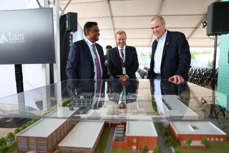
The photograph from the event shows Archer looking at a campus model with chief operating officer Sesha Varadarajan and Senator Jeff Merkley. Here, at least, the scale is forgiving. The work planned inside those buildings will be rather less so. Customers and Lam engineers are meant to develop processes together, with more room for experimentation.
His other laboratory investment returns the story to a smaller room. The Caltech teaching lab announced in 2025 was designed around undergraduate work, with microscopes, etching systems, deposition tools and characterization equipment. The equipment would let students make devices and examine the results. Archer’s remembered pleasure in a college class had found a concrete expression: another generation getting access to the tools.
There is something appealingly literal about that choice. After a career spent learning how to make increasingly complicated things, he helped provide a place where students could begin. A useful room, some demanding equipment, an idea ready to be tried. Plenty can happen from there.
Keep following the work
- Lam Research - company website ↗
- Tim Archer - LinkedIn ↗
- Tim Archer’s essays - Lam blog ↗
- The Archer teaching laboratory - Caltech ↗
- Archer’s Senate testimony - March 2022 ↗
- Selective etching and three-dimensional chips - Archer’s essay ↗
- Workforce development - Archer’s 2021 essay ↗
- GEM board appointment - September 2020 ↗
- Virtual fabrication training in India - June 2023 ↗
- Yongin campus and university collaboration - October 2024 ↗
- Sustainability letter - July 2023 ↗
- Oregon laboratory expansion - August 2026 ↗
- Listen: Archer on AI infrastructure - Bloomberg Talks ↗
- Watch: Archer with Jon Fortt - CNBC ↗
- Watch: Lam Research’s official YouTube channel ↗
LAM RESEARCH COMPANY ACCOUNTS