The awkward thing about a fast computer is that it can still be kept waiting. Its processors may be ready to work while the data they need is somewhere else, travelling through connections that cannot keep pace. Dr Jekaterina Viktorova has built a company around this inconvenience. She is interested in the small metal paths between chips, and in a deceptively practical question: could we make them another way?
Viktorova, usually called Jeka, is the co-founder and CEO of Syenta. Her background is chemistry, her doctoral speciality localized electrodeposition. Those words are unlikely to improve a dinner party. Yet they describe a route into one of the physical constraints facing AI: getting separate pieces of silicon to communicate efficiently. However clever the software becomes, its hardware still needs somewhere to put the wires.
Her career has followed that manufacturing question across countries and institutions. It took her from printed electronics in Germany to research in Canberra, then to a Sydney company with an American operation. The continuity matters. A fashionable application has arrived around a problem she was already pursuing. The problem was there before the funding announcements and before AI became everyone’s preferred opening sentence.
A printer at the kitchen table
Born in Latvia, Viktorova went to Germany to study chemistry. She earned a master’s degree at RWTH Aachen and worked in printed electronics before moving to Australia. At a German startup, the work included a sensor intended to detect whether fresh food had spoiled. It was an unglamorous application with a useful consequence: she encountered the difficulties of manufacturing the electronics themselves.
A sensor can be a good idea and an awkward object to produce. There are materials to choose, patterns to form and processes that must cooperate. Anyone hoping to build electronics cheaply and at scale eventually has to confront the tools. Viktorova’s later work keeps returning to that point. Making a device possible on paper is only part of the job; someone must be able to manufacture it.
In February 2019, she joined Professor Luke Connal’s research group at the Australian National University. The student-supervisor relationship became a collaboration that both described as a partnership from its beginning. Connal, a polymer chemist, sent her an idea by email one night. They tested it in the laboratory the following day. The first proof of concept worked.
A successful experiment has a pleasingly abrupt ending. A manufacturing project does not. The early result left years of refinement and development ahead. When access to the research laboratory was interrupted, Viktorova took the printer home. It occupied her kitchen table for months. “So I shared my kitchen with it for months,” she recalled. It is an unusually economical account of devotion to a project.
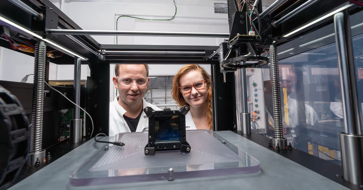
The kitchen is a revealing detail because it gives the research a physical address. We can talk about commercialisation as though it were a clean arrow between a university and a company. In practice, the equipment has to live somewhere, the experiments have to continue, and the person doing them has to arrange a life around the work. For Viktorova, that arrangement temporarily included sharing a domestic surface with a printer.
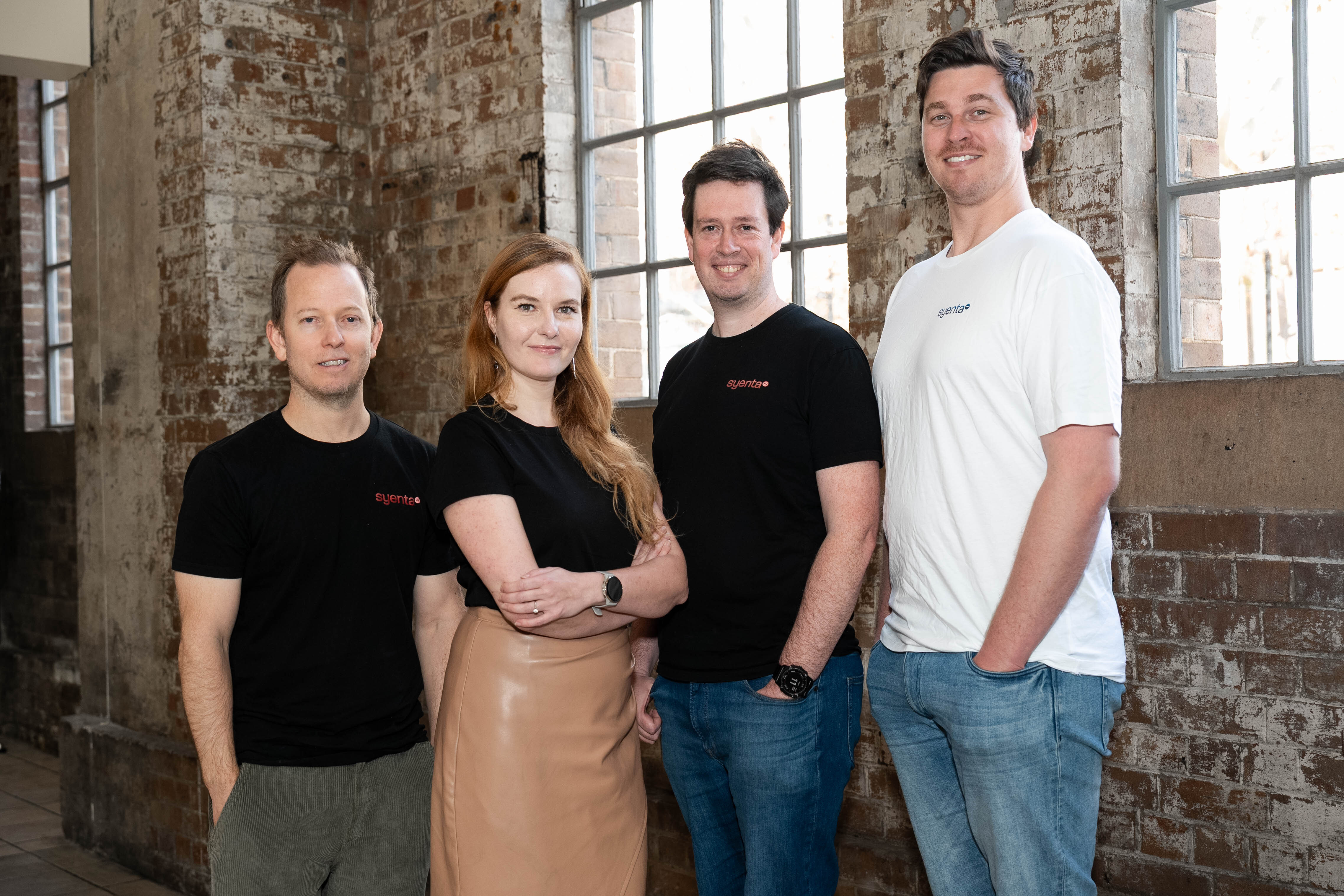
The project became Syenta, previously called Spark3D. The company was incorporated by 2022, with a founding group that included Viktorova, Connal, Ben Wilkinson and Zachary Dowse. Chemistry, materials science, applied physics and operating experience met in the same enterprise. A research partnership had become an organisation, with all the additional questions an organisation brings.
The chemistry of fewer steps
Electrochemistry provides the starting point for understanding her invention. Electroplating, familiar from metal finishes, uses electrical processes to deposit material. Syenta applies electrochemical manufacturing with control over where that material goes. Its current process, Localized Electrochemical Manufacturing, combines deposition and patterning in a single step, using a patterned stamp electrode to define the areas where metal is deposited.
In plain terms, the shape and the material arrive together. That is an appealing proposition in a business where the route to a finished structure can involve repeated stages of adding material and removing it. Each stage needs equipment, time and coordination with the next. A shorter route is valuable only if the result meets the requirements, but it is a sensible route to investigate.
The early ambition extended across printed electronics. A machine capable of working with different functional materials could help people prototype devices without outsourcing every iteration. Syenta’s early industrial customer GreatCell Energy used its printing methods in solar-cell development. That gave the research something concrete to answer to: a customer trying to make a device, with cost and fabrication questions of its own.
By March 2023, Viktorova was presenting electrochemical printing of multi-material electronics at TechBlick. The work could accommodate metals, semiconducting materials and polymers. That breadth helps explain why the story did not begin with a single AI product. The underlying interest was a manufacturing capability. Different devices could ask different things of it.
The present commercial focus is advanced semiconductor packaging. Chiplets are separate chips assembled to operate together; interconnects provide the routes between them. As systems combine more components, those routes become consequential. Better individual processors cannot automatically compensate for a connection that limits the movement of data. Think of a group of very efficient colleagues communicating through a very inefficient inbox.
Viktorova’s task is to make the manufacturing answer useful inside an existing industry. In her May 2026 CEO interview, she described customers starting with technical collaboration: establishing their requirements and evaluating how Syenta’s process could fit their packaging flows. The emphasis is practical. An interesting process needs to meet a customer’s production reality, which rarely has room for an interesting inconvenience.
Six weeks on the clock
The industrial ambition was present early. Blackbird’s December 2022 investment account described a benchtop printer and longer-term semiconductor questions. Could the printing reach smaller dimensions? Could it happen in parallel? These were explicit technical uncertainties, alongside an initial product with customers. The distant objective came with nearer experiments that had to earn their place.
Cameron Ferris, co-founder of Inventia, introduced Viktorova to Blackbird. His description of her as a “learn-it-all” is more useful than a generic founder compliment. A scientist becoming a chief executive has a considerable curriculum ahead: customers, hiring, financing and all the decisions that do not become easier because the chemistry is sound.
The December 2025 Wild Hearts conversation put a sharper edge on the financing chapter. Its account describes a period the previous year when Syenta had six weeks of cash remaining and no term sheets. Two weeks later, four offers were on the table. That chronology conveys pressure without needing an imaginary scene of anxious pacing or a conveniently dramatic telephone call.
“I’ve been just talking to people about what we do.”
Jeka Viktorova / Wild Hearts, December 2025
Her reflection on the conversation around funding was about speaking in a way that fitted the founder and the work. The line is almost disarmingly plain. A technical company can surround itself with elaborate explanations. Sometimes a useful starting point is to describe the problem clearly enough that the person listening can see why it matters. That still leaves the obligation to demonstrate an answer.
There is also a network behind the individual. Viktorova has spoken appreciatively of mentors around ANU and the Canberra startup community. In July 2023, she joined an ANU panel on taking research ideas to market. The collective discussion covered trusted teams, learning from failure and articulating a product’s value. Those concerns sit naturally beside her own journey from laboratory development to company leadership.
Sydney, Tempe, and the work ahead
In April 2026, Syenta announced an A$37 million Series A led by Playground Global and Australia’s National Reconstruction Fund. Former Intel chief executive Pat Gelsinger joined the board. These developments added financing and semiconductor experience around the company. They also moved Viktorova’s responsibilities further into the commercial and industrial relationships needed to develop the technology.
Funding announced for Syenta’s next stage of commercialisation. A round amount, rather than a measure of manufacturing performance.
That same month, the company announced its first US facility at ASU Research Park in Tempe, Arizona. The site is intended as a demonstration and development hub, including work on the Achyon LEM platform. Being closer to customers, research institutions and engineering talent gives an international expansion a practical purpose. A manufacturing company needs places where a conversation can turn into work on an actual process.
Viktorova has also stated an intention to keep the company’s research roots in Australia while it grows globally. That is a more specific ambition than simply becoming international. It connects the place where the work developed with the places where it may be adopted. Her own career already spans that geography: European study and industry experience, Australian doctoral research, and now operations reaching the United States.
The technical conversation continues elsewhere, too. In 2026 she presented Syenta’s approach at ISS Europe, where the discussion included resilient manufacturing and European industrial capability. Her public LinkedIn activity also announced an August presentation at SEMICON Taiwan on scaling additive copper interconnects for panel-level packaging. The audience has changed substantially from a university research group.
The remaining work is the important part of her present story. Syenta is advancing toward high-volume manufacturing and collaborating with the semiconductor ecosystem. Money can support those efforts; it cannot substitute for a process that performs where a customer needs it. The questions now concern scale, integration and repeatability, as well as the small structures themselves.
Viktorova began by confronting the tools available to make electronics. She is still confronting them, with a larger team and a more demanding application. The kitchen printer makes a good anecdote. The continuing manufacturing question gives it meaning. Somewhere between an idea for a device and a device that works, there is a connection somebody has to make.