The future of artificial intelligence may depend on an old urban problem: there is too much traffic and not enough road. Inside the newest computing systems, processors can perform astonishing arithmetic, yet they spend precious time waiting for data to arrive. Darius Bunandar has chosen to work on the road. His material is silicon. His traffic is information. His favored vehicle is light.
This is a less theatrical assignment than teaching a machine to write poetry or fold a protein. It is also the sort of assignment on which theatrical things depend. A large AI model is not trained by one omnipotent chip. It is divided across many processors, which must continuously exchange parameters and results. Their conversations consume energy, occupy physical space and slow down as the crowd grows. Faster calculators merely make the awkward silences between them more conspicuous.
At Lightmatter, the company he co-founded, Bunandar serves as chief scientist and a board director. His brief crosses photonic devices, electronic control, algorithms, packaging and the architecture of entire systems. He is not trying to decorate conventional computers with a few optical flourishes. The larger wager is that light can become part of their foundation: first as interconnect, then as a source and, eventually, as a means of computation itself.
An education in invisible forces
Bunandar's career makes more sense if read as a series of encounters with forces that cannot be seen directly. At the University of Texas at Austin, he studied both physics and mechanical engineering. One discipline supplied abstractions; the other insisted that abstractions eventually meet bolts, stresses and tolerances. He graduated with bachelor's degrees in both fields in 2013.
Before photonics became his trade, he briefly worked at BakerRisk in Texas as a blast-effects co-op engineer. The job involved large-scale blast experiments and simulations of explosions. Elsewhere, with the Caltech-Cornell Simulating eXtreme Spacetimes collaboration, he developed software to visualize how binary black holes affect light. The first subject was brutally tangible, the second cosmically remote. Both asked a young engineer to turn mathematics into a picture of what matter and energy would do next.
Then the scale collapsed from black holes to circuits. At MIT, under physicist Dirk Englund, Bunandar studied quantum cryptography and communication using compact nanophotonic devices. He contributed to a demonstration of metropolitan quantum key distribution built on silicon photonics, published in 2018. In an intercity field test, the system generated secret keys across 43 kilometers of fiber. The point was not that light could travel. Everyone knew that. It was that subtle quantum information could be created, controlled and read by devices made on a scalable chip platform.
experiments
visualization
communication
interconnects
That work established a pattern. Bunandar does not belong neatly to one layer of the technical stack. He moves between physical behavior, mathematical models, manufactured devices and complete systems. It is a useful disposition in photonics, where a beautiful optical effect can be rendered useless by a packaging problem, an unstable laser or control electronics that demand too much power.
The check was large. The lesson was larger.
In 2017, Bunandar joined his MIT lab colleague Nicholas Harris and Sloan student Thomas Graham in an entrepreneurship class. Their premise was audacious but legible: use optical circuits to perform the operations at the heart of machine learning. Under the name Lightmatter, the team entered MIT's $100K Entrepreneurship Competition and won its $100,000 grand prize.
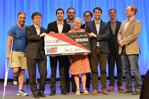
The photograph is classic startup archaeology: a ceremonial check, a blue curtain and a collection of people whose technology is easier to admire than explain. The money had obvious uses. The team planned to meet potential customers, rent its first office and visit manufacturers. Yet Bunandar later described the less visible capital supplied by MIT Sandbox. Mentor Dan Gilbert helped the founders understand their first term sheet, negotiate fundraising and frame the technology as a product.
“When bringing an early-stage technology to the market, it is not only about solving hard problems but also about evangelizing the technology or the solutions to customers.”Darius Bunandar, on MIT Sandbox mentorship
“Evangelizing” can sound like a license for noise. In Bunandar's account it means translation: identify the customer's constraint, then make the physics answer it in terms that survive outside the laboratory. The distinction helped Lightmatter move from a promising optical accelerator to a broader stack of products. Envise performs matrix operations with light. Passage addresses communication between chips. Guide supplies and controls the lasers that photonic systems require. The product names are concise because the engineering underneath them is not.
The edge of the chip is a bad neighborhood
The problem Bunandar now emphasizes is geometric. Conventional input and output crowd around the perimeter of a chip package. Engineers call this boundary the shoreline, an amiable word for a stubborn limit. A larger processor needs more bandwidth, but its edge does not grow as quickly as its appetite. Electrical signals also lose efficiency over distance. At data-center scale, the bill arrives in watts, latency and expensive processors waiting idle.
Lightmatter's Passage architecture changes the floor plan. It places a photonic interposer beneath compute and switching chips, using 3D integration so optical communication is no longer confined to the rim. In the company's M1000 platform, that substrate is a network: a 4,000-square-millimeter silicon complex with 34 chiplets, 1,024 high-speed electrical lanes and 256 fibers, designed for as much as 114 terabits per second of bandwidth. The numbers are impressive. The arrangement is the real idea.
If connections can leave only from a package's edge, bandwidth is constrained by perimeter. Put a photonic layer beneath the chips and the available connection area becomes the surface, not merely the border.
Bunandar has put the point plainly: communication still happens on the chip perimeter, and there is not enough shoreline to scale bandwidth. This is the rare metaphor that improves when taken literally. The valuable real estate in AI hardware is measured in fractions of millimeters, and a traffic jam can occur before data has crossed a circuit board.
His August 2025 technical essay tackled another piece of real estate: the fiber itself. Lightmatter demonstrated a bidirectional link carrying 16 wavelengths over one standard strand. Conventional optical links often dedicate separate fibers to each direction. Sending traffic both ways, across many colors of light, can reduce the number of fibers while increasing the number of connections available to a switch or processor. It is a modest-looking physical change with architectural consequences. Fewer fibers can mean denser systems, fewer network hops and less time spent moving model data through slower routes.
Watch Bunandar explain large-scale AI with photonicsThe scientist becomes an integrator
The chief scientist in this story is not a solitary keeper of theory. Public descriptions of Bunandar's role repeatedly use the language of coordination: research in architectures and algorithms, the joining of silicon photonics with advanced packaging, and system-level design. His publication record follows the same widening arc. There is quantum-secure metropolitan communication, an electro-photonic accelerator for deep neural networks, an analysis of the carbon footprint of photonic computing, and a 2025 commentary on quantum photonic machine learning.
That range also keeps the environmental promise honest. Light can perform some operations and carry information efficiently, but a photonic chip still has to be fabricated, packaged, powered and controlled. Bunandar co-authored lifecycle research that modeled those costs rather than treating photons as environmentally immaculate. Every technology looks clean if its boundaries are drawn tightly enough. Systems work begins by drawing them wider.
By 2026, his public talks had moved decisively toward infrastructure. At Photonics West he joined a discussion on co-packaged optics for data centers. At the European Conference on Optical Communication, his title put “interconnect and memory bandwidth before computation.” A scheduled SEMICON West presentation carries the argument into energy: optical links, dense wavelength division and industry collaboration as tools for bending AI's power curve.
There is a pleasing inversion here. Bunandar's doctoral work concerned secrets encoded in light. His present task is to make the machinery of light routine, manufactured and interoperable. It must work across foundries, packaging lines, laser sources, fibers and the chips of other companies. The physics may be elegant; the ecosystem is gloriously untidy.
The next breakthrough in AI hardware may look less like a brilliant new brain than a city whose roads finally match its traffic.
Lightmatter's original competition pitch centered on optical computation. Its current emphasis on interconnects is not a retreat from that ambition. It is an ordering of obstacles. Before a machine can calculate at vast scale, it must feed its processors and let them talk. Bunandar's career has prepared him for precisely this kind of sequence: understand the force, map the system, solve the constraint that is actually in front of you.
Explosions taught him to model violent energy. Black holes taught him to visualize distorted light. Quantum communication taught him to control fragile information on silicon. Entrepreneurship taught him that even excellent science needs a buyer who understands the benefit. In the data center, those lessons meet. The result is not a ray of light racing heroically through a machine. It is something more useful: an engineered network in which millions of quiet journeys arrive on time.