A Swiss watch seems an unlikely place to look for a semiconductor company. There is no server rack on the wrist, no charging cable attached to the movement. Yet IceMOS supplies silicon materials for precision watch components. A business built around wafers and microscopic structures found customers among people whose product measures time with mechanical parts.
- Custom silicon wafers for sensors, circuits and precision components.
- Power switches built using silicon and MEMS process expertise.
- A $22 million funding round in 2025; a Hong Kong support office followed.
The watchmaker’s detour
The Department for Business and Trade’s account of IceMOS describes the watch business as an unexpected destination. Word spread that the company could help watchmakers move from steel to silicon. The important detail is the method: work closely with a customer on something that the catalogue does not already contain. The unusual application followed the ability to make a particular structure.
Founded in 2004 by Samuel J. Anderson, IceMOS has accumulated experience in bonding wafers, etching deep into silicon and controlling its shape. Anderson’s management biography lists fourteen years at Motorola before IceMOS. The resulting business sits upstream of many finished products. Its customers need the right starting material, sometimes with difficult work already performed inside it.
Start with the layers
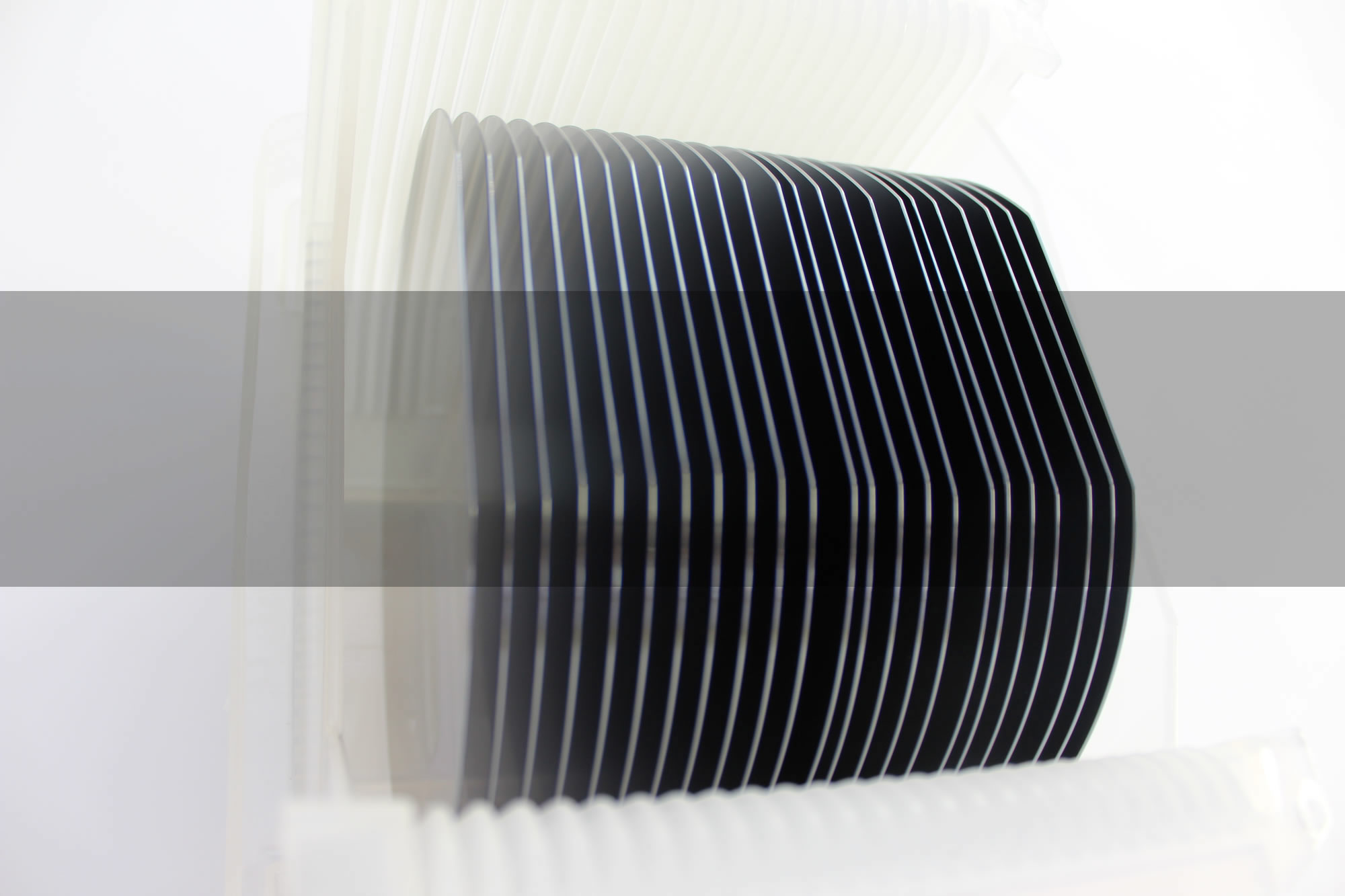
Take silicon-on-insulator, or SOI. The name is an unusually helpful piece of semiconductor vocabulary: a working silicon layer sits above an insulating layer, supported by a thicker wafer. IceMOS supplies thick-film SOI in diameters from 100 to 200 millimetres. Customers can select parameters for applications including MEMS, optical devices and analog circuits. The wafer is part of the engineering decision.
For a pressure sensor or microphone, the useful feature might be a cavity beneath a membrane. IceMOS’s cavity-bonded SOI embeds pre-etched features under silicon. Its product description points to simpler manufacturing flows and reduced stiction at release. Stiction is a wonderfully small word for an awkward problem: tiny structures can stick when they should be free. Building the cavity into the starting substrate changes the manufacturing sequence.
Other customers need electrical separation. Trench-SOI combines insulating layers with deep etched trenches and refill to isolate components on the same chip. Through-wafer interconnect substrates tackle another problem, delivering connections already formed through the material. For each customer, the conversation begins with what the finished device needs to do. The substrate can then carry some of that burden.
This creates several ways to buy from IceMOS: stock wafers, customised substrates, power devices, or individual foundry processes on customers’ own wafers. Inspection is another service. Scanning acoustic microscopy examines bonded interfaces without destroying them. These are practical purchases for manufacturers who have a design and a specific gap in their production capabilities.
The direct-bonded SiSi range makes the point another way. It joins silicon layers whose resistivity and crystal orientation can be selected for the application. IceMOS offers these wafers as an alternative to thick epitaxial layers for devices such as power components and detectors. The business is selling control over the starting conditions.
The switch is the other half
Now move from sensing to power. A MOSFET is a transistor used here as an electrical switch. IceMOS combines MEMS manufacturing techniques with silicon superjunction structures in its mSJMOS platform. Its stated aim is improved power efficiency. The appeal of this approach is straightforward: apply sophisticated structures and processing to a material with an established manufacturing history.
There are alternatives on both sides of the business. Infineon sells CoolMOS superjunction devices; Soitec offers MEMS-SOI substrates. IceMOS’s distinguishing proposition is the combination of customised wafer engineering and its MEMS-based power-device approach. A designer still has to compare the actual specifications. A clever structure earns its place by working in the intended product.
Silicon does not settle every problem. IceMOS’s own technical writing describes extending its research to a silicon-carbide engineered drain after assessing high-voltage requirements. A 2021 NASA project supported radiation-tolerant transistor development. Spacecraft introduce a demanding variation on the power-supply problem: efficiency must coexist with survival in a harsh radiation environment. That research is a separate engineering task from selling a standard switch.
Capital meets the factory floor
In April 2025, IceMOS announced a $22 million Series E at a $110 million post-money valuation. Investor 57 Stars committed $7.5 million. The intended uses included manufacturing expansion, device design and commercial capabilities as the company prepared its mSJMOS platforms. Those figures describe financing and plans, rather than the price of a wafer or proof of a completed rollout.
“Our sensing and power technologies are paving the way for more energy-efficient and CO2-saving solutions that support decarbonization.”
Samuel J. Anderson · April 2025
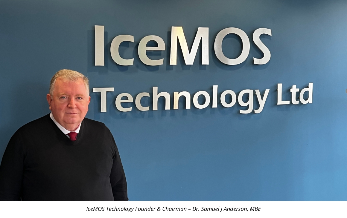
The organisation crosses several borders. Headquarters is in Paradise Valley, Arizona; Belfast houses manufacturing, and Tokyo supplies design capability. In December 2025, IceMOS added a Hong Kong Science Park office for sales, applications engineering and supply-chain support. That is a concrete extension of the business: customers in Asia gained a regional point of technical and commercial contact.
Its place in the market became particularly clear in the UK government’s September 2026 semiconductor study. The report identifies IceMOS as one of the country’s few dedicated small-volume foundry service providers. Small volumes can still demand exacting work. A specialist customer may need a process that a much larger supplier has little reason to accommodate.
The export record supports that specialist position. In 2024, IceMOS reported that 99 percent of its business went outside the British Isles, and it won the manufacturing category of the government’s Made in the UK, Sold to the World awards. An unusual specification can have a geographically scattered market. Reaching it becomes part of the manufacturing business.
Borrow the question
There is a useful habit here for other businesses: ask which awkward step a customer would like somebody else to solve. IceMOS’s range suggests answers in cavities, isolation, interconnects and wafer inspection. The transferable idea is to build around a production constraint, then look for another industry with a related constraint.
For a prospective buyer, the next step is specific: define the wafer dimensions, layer requirements, operating conditions and processing work needed. Compare those with the supplier’s capabilities and the finished device’s qualification requirements. The approach is useful when custom structure solves a real problem. Where a standard material already meets the need, extra engineering has to justify its cost. Even a watchmaker knows when to stop adding parts.