Holography has spent half a century loitering just offstage, waiting for its cue. The audience knows the scene already: a small blue princess, an urgent message, light behaving as if it had substance. Mike Noonen knows the scene too. At a meeting during CES 2025, he reached for Princess Leia within roughly a minute. It was an efficient way to explain both the appeal and the problem. Everyone recognizes the promise. Almost nobody has seen the promise become an ordinary product.
Noonen’s career has been an extended education in how difficult technologies become ordinary. He started as an electrical engineer, worked on early video communications, moved through networking and semiconductor companies, helped repair large operations, advised startups, built an incubator and led a millimeter-wave chip company to an acquisition. When he joined Swave Photonics as CEO in 2022, the assignment was familiar in shape even if the physics was novel: take a laboratory advantage, give it a market, and keep the company alive long enough for the two to meet.
Today, Swave lists Noonen as an adviser and co-founder Theo Marescaux as interim CEO. The change makes his period in the chief executive’s chair easier to see as a chapter. During it, Swave introduced its Holographic eXtended Reality platform, demonstrated a full-color prototype, earned CES recognition, closed a €27 million Series A and added a €6 million follow-on. The less visible work was translation. Holography had to stop sounding like a movie prop and start sounding like a product roadmap.
Origin signalA kid from Colorado learns to translate
Noonen studied electrical engineering at Colorado State University. His early job at NCR Microelectronics put him close to customers as a field applications engineer teaching mixed-signal ASIC design. That role sits at a useful border. An engineer must understand the circuit, but also the confused person holding the data sheet. Translation was not ornamental. It was the work.
He carried that instinct into 8x8, where he held sales and general-management roles and appeared as an inventor on patents involving home videoconferencing, internet telephony and even browsing the web through a telephone interface. The documents now read like artifacts from an era when a video call was an engineering project rather than a calendar link. They also reveal an enduring preoccupation: how machines mediate human communication.
Cisco followed, then National Semiconductor. In 2001, at 38, Noonen was named to run National’s wired communications division, responsible for copper networking, optical links and communications interfaces. Seven years later he moved to NXP as executive vice president of worldwide sales and marketing. In 2011 he joined GlobalFoundries with an unusually broad remit across products, quality, design, sales and marketing. The title is almost a sentence, but the logic is clean. In chips, the product cannot be separated neatly from the process that makes it.
The hard thingWhen venture capital feared silicon
By 2014, the semiconductor startup had become a peculiar creature: essential to the future, awkward in a pitch meeting. Chips required expensive design software, specialized fabrication, packaging, validation and patience. Software had trained investors to admire lighter appetites. Noonen supplied the joke that stuck: Sand Hill Road treated silicon like plutonium.
His answer was Silicon Catalyst, co-founded with fellow industry veterans. The incubator assembled an ecosystem around young chip companies: design tools, foundry access, mentors, industry partners and investors. Its point was not to make hardware cheap. It was to make the expensive uncertainties arrive in a more survivable order. The organization received an EE Times and EDN startup award in 2015, a pleasingly recursive result for an incubator whose product was other startups.
“Raise your hand and volunteer, get involved, cultivate your network, and good things will happen.”Mike Noonen, advice to aspiring entrepreneurs
The line sounds breezy until placed beside the machinery of a semiconductor company. A network here is not a stack of business cards. It is the foundry contact who explains a constraint early, the tool vendor willing to help, the board member who has seen a failure before, the customer prepared to test a rough device. Noonen’s career accumulated those relationships while he served on boards, advised companies including SiFive and Mythic, became interim CEO of Ambiq Micro and helped Silego before its acquisition by Dialog Semiconductor.
His other maxim was shorter: cash is king. Hardware turns cash into evidence slowly. A prototype may take months to return from fabrication, and it can return bearing bad news in microscopic form. Frugality is not timidity in that setting. It is the purchase of another learning cycle.
A repeatable patternResearch, runway, result
MixComm offered a concentrated test of that philosophy. The company drew on years of radio-frequency research at Columbia University and earlier public investment in RF silicon-on-insulator. Noonen joined as CEO in 2019. MixComm built millimeter-wave components for 5G and reached a sale to Sivers Semiconductors in February 2022. The outcome looked quick only if one began the clock when the company did. Noonen insisted on the longer view: the commercial product rested on research, process development and institutional memory accumulated well before incorporation.
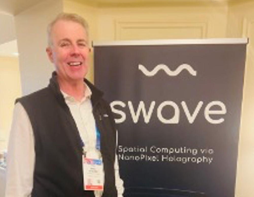
This is the pattern that made Swave legible to him. The company spun out of imec in Belgium after more than a decade of research. Its core proposition is a spatial light modulator made with extremely small pixels and established semiconductor processes. Rather than merely displaying a flat image, the device shapes light so that a digital object can occupy depth. The initial commercial emphasis became compact augmented-reality glasses, with other display formats behind them.
The technical phrase is pixel pitch. Reduce the distance between pixels far enough and the display can steer light across useful angles while retaining resolution. Swave describes pixels below 300 nanometers, fabricated on CMOS. Noonen’s favorite explanation joined materials science and display technology by way of candy: the photonic equivalent of a Reese’s Peanut Butter Cup. It is hard to picture phase-change material. Peanut butter and chocolate require less preparation.
The pixel gets a business planFrom spectacle to milestones
Noonen did not invent Swave’s technology. His contribution was to make its progression understandable to people who allocate money, build systems and buy components. The sequence became concrete. Launch the platform. Show color. Produce prototype silicon. Put development hardware in front of prospective customers. Hire optical, engineering and financial leadership. Fund the next pass.
In a 2025 conversation, he identified the first-pass success of Swave’s Onyx prototype as the company’s pivotal milestone: 256 million nano-pixels on a small CMOS die. “First pass” carries a special sweetness in chip design. It means the expensive journey through fabrication returned working evidence without demanding an immediate do-over. The phrase is modest. The avoided bill is not.
Funding supplied the runway. The €27 million round announced in January 2025 was followed in June by €6 million from IAG Capital Partners and Samsung Ventures. Noonen framed the money around commercialization, applications and a collision between spatial computing and AI. The rhetoric had shifted from the metaverse language of 2022 toward useful eyewear and displays. Markets rename their dreams. Engineers still have to tape out the chip.
What compoundsThe operating system beneath the résumé
Noonen’s résumé can look restless: large companies, young companies, boards, interim assignments, an incubator. Read as a system, it is more consistent. He goes where technical advantage needs organizational leverage. At National, NXP and GlobalFoundries, that meant aligning product, sales and manufacturing. At Silicon Catalyst, it meant building shared infrastructure around founders. At MixComm and Swave, it meant converting accumulated research into milestones a market could recognize.
The useful lesson is not to copy his industry. It is to notice the sequence. Begin with differentiation strong enough to matter. Surround it with people and institutions that shorten the wrong turns. Conserve enough cash to survive the learning. Explain the technology in language that can travel without flattening it into nonsense. Then repeat.
His public advice about volunteering belongs in that sequence. Ecosystems are built before anyone urgently needs them. A favor offered in one cycle becomes context in another. It is easy to call that networking and miss the more demanding word: participation.
Holography remains a future-tense business. Swave has prototypes, financing and a technical argument; the broad market still has to arrive. Noonen, now in an advisory role at the company, has left behind a cleaner bridge from the cinematic image to the semiconductor die. On one side, light floats in the room. On the other, 256 million tiny pixels wait for a customer. Between them sits the work of making wonder repeatable.