Before Fab2, there was a transistor that needed too much encouragement. Sam Zeloof’s early homemade chips used aluminum gates and required high voltages. They worked in a guitar distortion pedal and an LED blinker, but demanded one or two nine-volt batteries. For a young engineer trying to make useful silicon, that was a rather inconvenient definition of success.
- Fab2 builds chipmaking tools and wants to manufacture complete compact fabs.
- Studio puts collaborative chip design in a browser.
- A $500 million Series A funds the ambition; reliable manufacturing remains the test.
A chip layout made in Photoshop
In 2021, Zeloof documented a different approach. Switching to polysilicon gates brought his transistors into the neighborhood of ordinary low-voltage logic. He had already made a six-transistor integrated circuit in 2018. Now he was testing arrays of 100, with 1,200 transistors on one piece of silicon. For the simple layout, he used Photoshop. The semiconductor industry had acquired a most unlikely drafting room.
The write-up is revealing because it includes the untidy parts. Some transistors shorted to the underlying silicon. Some chips were only partly functional. Zeloof acknowledged compromised yield and repeatability. He also found a workaround: buy wafers with difficult layers already deposited. A lot of 25 wafers cost $45 on eBay. That was a materials bargain, not the price of the laboratory.
“Of course, yield and process repeatability are diminished.”
Sam Zeloof, documenting his homemade Z2 process, 2021
The experiment suggests a useful distinction. Making a transistor work establishes possibility. Making the next thousand behave similarly establishes a process. Fab2, the company Zeloof founded with chip architect Jim Keller, inhabits the distance between those achievements. Keller brings experience from designs including Apple’s A4 and AMD’s Zen. Zeloof brings the habit of asking which expensive step can be simplified.
The factory gets a product number
Originally called Atomic Semi, the venture adopted the Fab2 name in 2026. The name is almost an instruction manual: build a fab that builds fabs. Its intended output includes the machinery and infrastructure of semiconductor production, alongside the chips. A factory normally sits behind the product. Here, the factory is supposed to become something the company can reproduce.
This requires an unfashionably long shopping list. Fab2 designs components, assembles them into machines, and combines those machines into fabs. Pumps, valves, gas lines, chambers, sensors and precision actuators all enter the picture. Its explanation is disarmingly practical: the components it wants do not exist, so it makes them. Vertical integration becomes a response to a particular engineering requirement.
- 01ComponentsPumps · valves · sensors
- 02MachinesFabrication tools
- 03FabsComplete production systems
That choice also creates obligations. Every part brought inside becomes another part to design, test and manufacture. The potential advantage is control: a team can change the machinery when the process demands it. The practical question is whether those changes produce a repeatable system without making its maker responsible for an unmanageable collection of problems.
Three addresses for one industrial idea
Fab2’s footprint gives the plan some physical grammar. Austin has a 120,000-square-foot chip fab for research and production. Lockhart has a 30,000-square-foot fab fab, described as growing. San Francisco retains a 25,000-square-foot garage fab. The last name survives, although the building has considerably outgrown the domestic meaning of garage.
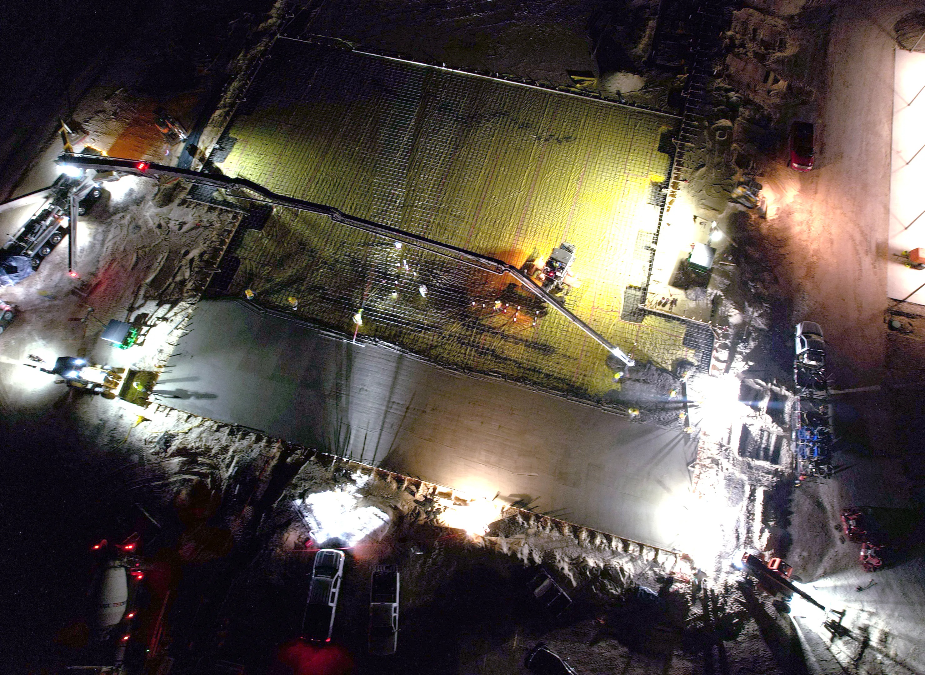
These sites represent different kinds of work: making chips, making the systems that make chips, and continuing development in the original city. Floor area is evidence of an industrial undertaking. It does not tell us how many customers have received equipment, how many chips pass inspection, or how cheaply the next factory can be built.
A browser tab belongs in the machine shop
The software project follows the same logic. Studio is Fab2’s browser-based, collaborative electronic design automation tool, covering layout, schematics and simulation. If fabrication becomes faster, the company reasons, design must keep pace. A quick machine loses much of its advantage when the drawing that feeds it moves through a cumbersome workflow.
For an engineering team, the attraction is a shorter route from an idea to something measurable. Designers can work together on the circuit rather than treating software as a separate island. Studio is part of the company’s development program; its description should not be mistaken for a published subscription offer or a promise that every browser user can order a chip tomorrow.
Half a billion dollars buys an attempt
In September 2026, Fab2 announced a $500 million Series A at a $3.7 billion valuation. Fundomo led, with investors including Naval Ravikant, Paradigm and Duquesne Family Office. The SEC’s offering record uses different accounting: $556.02 million sold, including $88 million in converted securities. Those figures describe overlapping financing, not two windfalls to add together.
Series A financing. Capital raised is not the cost of a fab.
The distinction matters. Financing buys engineering time, equipment and room to attempt the plan. Valuation records investor expectations. Neither measures the cost of producing a working customer chip. Fab2’s business is developing manufacturing infrastructure for other businesses; the economics will depend on equipment performance, utilization and the work its customers need done.
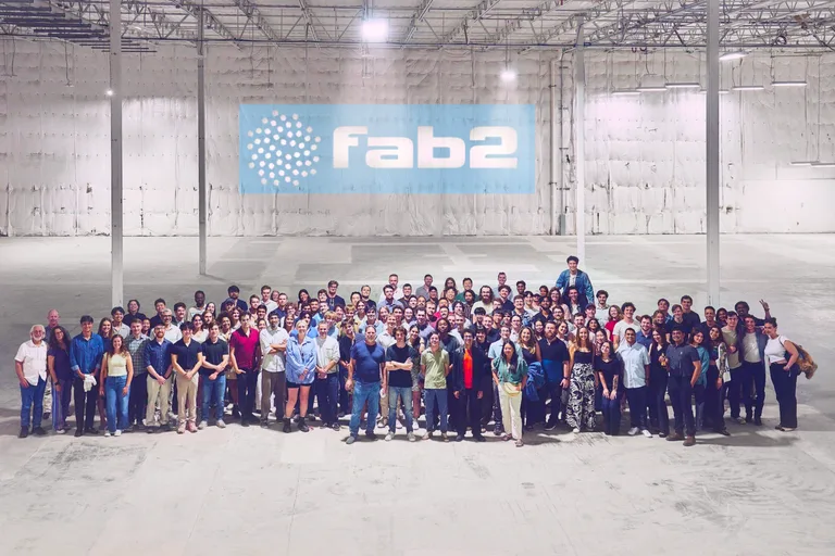
The recruiting language favors hands-on builders. Current roles cross electrical design, lithography research, process development, robotics software and production. That mix makes sense: a manufacturing fault does not politely remain inside one discipline. A sensor reading can become a firmware question; a firmware question can become a mechanical redesign.
The customer who values another try
The natural prospective user is a chip team that values another experiment sooner: researchers, designers and engineers working through small runs. That is a market argument, rather than a list of customer wins. Conventional foundry prototyping remains an alternative. Established equipment suppliers and EDA vendors occupy other parts of the workflow Fab2 is bringing together.
The approach must still meet the customer’s process requirements. High-volume production rewards throughput, consistency and qualified results. Faster experimentation alone cannot satisfy those demands. The lesson worth copying is narrower: identify the step that makes learning expensive, simplify it, then measure the defects honestly. The $45 wafers were an ingenious shortcut. What Fab2 must manufacture now is the confidence to repeat.