A chip factory is a peculiar place to look for a public utility. It buys electricity, purified water and process gases by the river. But the light that prints its most intricate circuits arrives differently: each extreme-ultraviolet lithography scanner carries its own highly specialized source. xLight has proposed a change that sounds almost impolite to this arrangement. Move the light source outside the fab. Make one machine serve many.
- xLight is developing a free-electron laser, or FEL, to supply EUV light for advanced chipmaking.
- Its planned system sits outside the fab and is designed to serve up to 16 scanners.
- The company raised $40 million in Series B equity in 2025 and received a finalized $150 million federal incentive award in 2026.
- The first prototype is planned for Albany, New York, with use at the Albany Nanotech Complex expected to begin in 2028.
The idea is less about inventing a new kind of chip than changing a factory bottleneck. EUV light exposes the tiny patterns on silicon wafers. More useful light can permit higher doses or faster exposure; that can mean more wafers through an expensive scanner. Current production EUV systems generate that light by firing lasers at tin droplets to make plasma. xLight wants to use electrons accelerated through magnetic structures instead. The light would travel from a central facility to the scanners that need it.
A chandelier for a factory
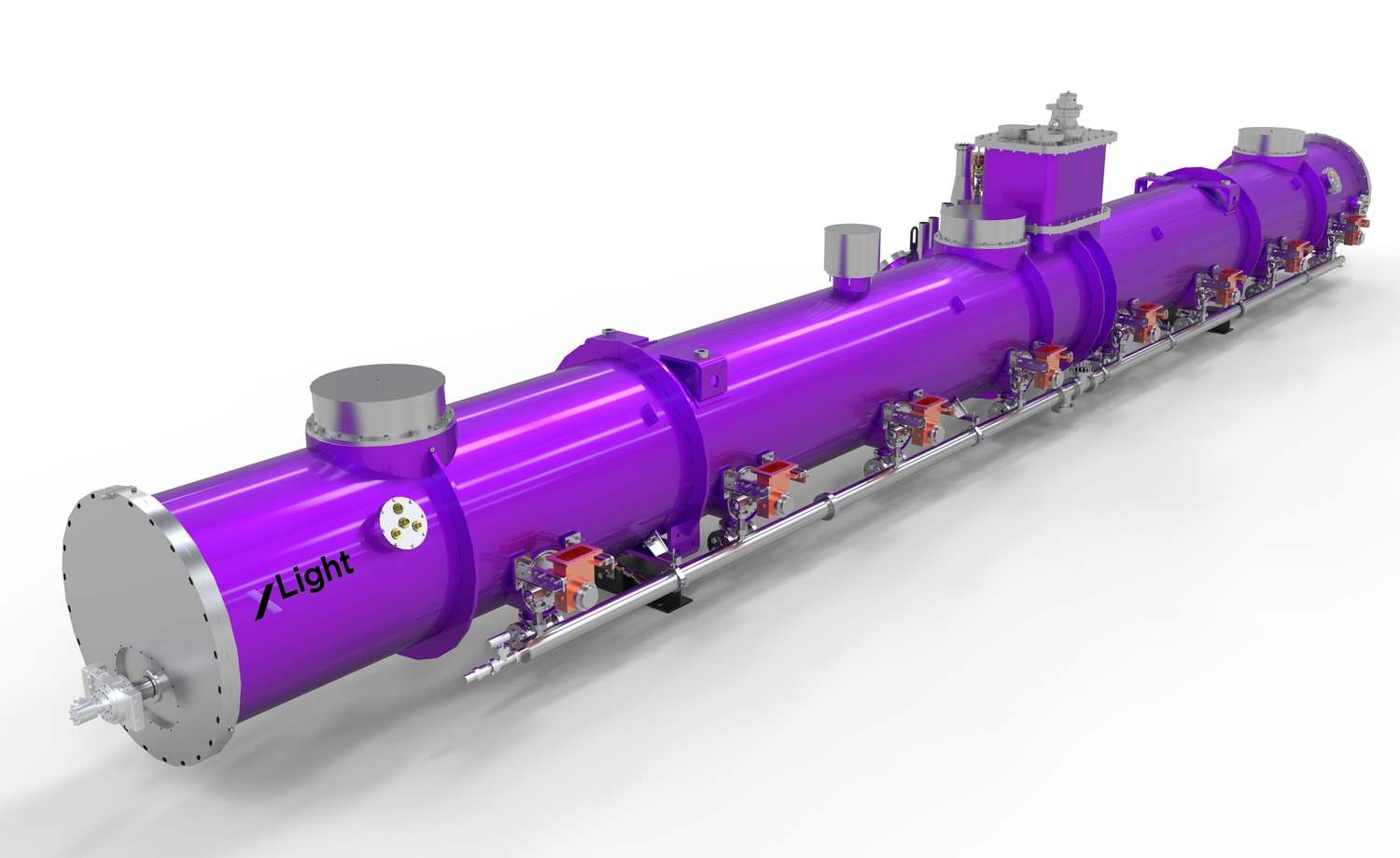
It helps to picture a chandelier, although xLight’s engineering drawings contain more magnets than crystal. A single source feeds branches. In the company’s plan, the accelerator and FEL sit outside the cleanroom, where space is costly and cleanliness is everything. An optical distribution network routes EUV light to multiple lithography tools. xLight says the architecture can support up to 16 scanners at once. The beauty of the proposal is the shared source; the headache is the same thing. When one machine becomes a utility, everyone notices when it stops.
That places xLight in a precise corner of the market. It is a prospective supplier of light-source infrastructure to advanced semiconductor manufacturers, rather than a chip designer or a maker of whole lithography scanners. Its natural customer is a fab operator with several EUV tools and enough scale to make centralized light attractive. Public announcements name research partners, but no production fab customer. Commercial pricing and contract terms have not been disclosed.
The national-lab shopping list
Founder and CEO/CTO Nicholas Kelez spent two decades in the U.S. national laboratory system. At SLAC, he was chief engineer for the Linac Coherent Light Source, a three-mile X-ray free-electron laser facility. That résumé explains both the ambition and the problem. Scientific FELs exist. A chip fab runs around the clock and measures success in throughput, yield and uptime. The leap is from a facility built for experiments to a source that operators can treat like a utility.
xLight’s partnerships read like a parts list for that leap. Fermilab is working with the company on superconducting radio-frequency cavities and cryomodules. Cornell’s CLASSE is collaborating on high-brightness electron sources, cavities and energy-recovery linac designs. Los Alamos is applying machine learning to accelerator diagnostics and automation. The last item sounds modest until one considers the operating schedule: xLight says continuous, 24/7 operation is a requirement of its technical roadmap. A factory cannot plan its work around a physicist’s shift.
“Lithography innovation is the key to reviving Moore’s Law.”Nicholas Kelez, June 2026
The company has also recruited semiconductor insiders. Former Intel chief Pat Gelsinger became executive chair in March 2025. Former GlobalFoundries CEO Thomas Caulfield joined the board in June 2026. Those appointments do not establish customer adoption. They do give the accelerator team people who know what factory operators will ask when a proposed breakthrough arrives at the gate.
The bill, and the bigger bill
The money attached to xLight has two different meanings. In July 2025 it closed a $40 million Series B led by Playground Global, joined by Boardman Bay Capital Management, Morpheus Ventures, Marvel Capital and IAG Capital Partners. Kelez said that round would complete detailed design and begin construction of a full-scale prototype. In December 2025, the U.S. Department of Commerce signed a letter of intent for $150 million in CHIPS incentives. The award was finalized in June 2026 with NIST. It supports construction and demonstration of the first FEL prototype at Albany Nanotech.
These sums are not a price tag for a commercial installation. They are a measure of the test still required. xLight argues that its system could produce four times more EUV power, cut the EUV portion of wafer cost in half, and lower total wafer cost by 20%. These are company projections. The interesting number for a customer will be the verified cost per good wafer after the system operates at scale, with maintenance, redundancy, optical losses and scanner integration included.
Each scanner has an integrated laser-produced-plasma source. Light comes from tin droplets struck by lasers.
An accelerator-driven FEL outside the fab sends tunable light through shared optical distribution to a fleet of scanners.
The incumbent does not stand still. ASML continues developing its plasma-based EUV source and has demonstrated a 1,000-watt source concept. xLight therefore must show an advantage against future versions of today’s technology, not only against the equipment already on factory floors. The attraction of its design is broader than raw wattage: removing tin and hydrogen consumables, tuning the light, and distributing it across tools could change operating economics. Each benefit, though, depends on reliable delivery at the scanner.
What the Albany machine must prove
xLight’s first prototype is planned for the Albany Nanotech Complex in New York. NIST describes the award as support for construction and demonstration; xLight expects to begin using the prototype there in 2028. That is the point at which a handsome diagram starts to meet less glamorous questions. Can the accelerator run continuously? How much EUV reaches the scanner after its journey through the optics? Can one source be serviced without stopping a line of tools? Do the predicted wafer savings survive a real fab’s accounting?
The visible sequence runs through design work, component collaborations, a large equity round and a federal prototype award. The practical lesson is transferable even outside chipmaking. When a mature industry treats a scarce input as a feature of each machine, ask whether it would work better as shared infrastructure. Then test the entire delivery chain, not merely the machine at the center.
The conditions are demanding. A fab with only one EUV scanner has less to gain from a central source. A multi-scanner fab may hesitate if shared downtime can stop every tool. Higher power is useful only if optics, masks, resists and scanner interfaces can use it. For now xLight has an architecture, serious partners and funded prototype work. The factory utility remains a proposition. Albany is where it must become a machine.