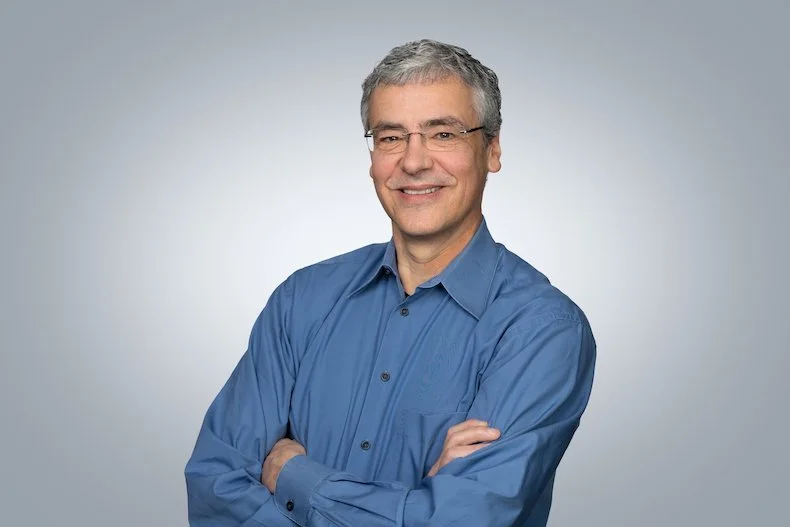
In 1997, a freshly minted PhD from the University of Michigan showed up at Lawrence Berkeley National Laboratory with a mandate that would have seemed absurd to anyone outside a handful of government labs: help build a working scanner that uses light with a 13.5-nanometer wavelength - shorter than a strand of DNA - to print semiconductor circuits. Patrick Naulleau did exactly that.
Nearly three decades later, the tools Naulleau helped invent are now running in semiconductor fabs from Taiwan to Germany. ASML's EUV machines - the ones that cost roughly $200 million each and are required to manufacture the world's most advanced chips - sit atop a technical lineage that runs directly through the Berkeley programs Naulleau helped build. He didn't leave when the hard part was done. He stayed, built more, and then decided the next hard problem was making sure those machines actually worked.
From the Lab to the Factory Floor
In August 2022, Naulleau stepped out of Berkeley Lab's Center for X-Ray Optics - which he had directed since 2010 - and into the CEO seat at EUV Tech Inc. The company, headquartered in Martinez, California, makes precision measurement instruments for EUV lithography: the tools that tell chipmakers whether their masks, pellicles, and resists are performing the way physics says they should.
It's not a pivot. It's a translation. For 25 years at LBNL, Naulleau's group built the instruments; now his company sells them. The underlying science - how extreme ultraviolet light interacts with materials, how phase errors in masks propagate to defects in chips, how you measure what you can't see with ordinary optics - is the same work he's been doing since the Clinton administration.
"At-wavelength metrology is critical for understanding and controlling the materials used for mask and patterning in EUV."
- Patrick Naulleau, CEO, EUV Tech Inc.What changed is the stakes. When Naulleau was publishing papers at Berkeley, a missed measurement meant a revised journal article. At EUV Tech, a missed measurement in a customer's fab means a batch of wafers worth tens of millions of dollars printing the wrong pattern - or a factory that can't ramp because nobody can explain why yield is low.
The SHARP Years: Building What Didn't Exist
Before EUV Tech, Naulleau's most visible instrument was SHARP - the SEMATECH Berkeley Actinic Inspection Tool. Co-developed with Berkeley Lab colleagues, SHARP was the world's first high numerical aperture EUV mask microscope. It used synchrotron radiation at the same 13.5nm wavelength as production scanners to inspect photomasks - the glass templates that define each layer of a chip - for defects that only show up when light actually hits them at operating wavelength.
Conventional defect review tools use different wavelengths or electrons. They work for many things. But for EUV masks, the patterns are so small, and the phase effects of thin-film interference so pronounced, that you genuinely cannot predict what a defect will do to the printed image without illuminating the mask with EUV itself. SHARP made that possible. The fact that it required a particle accelerator to operate tells you something about where the field was when Naulleau built it - and where EUV Tech is now trying to take it.
EUV light at 13.5nm cannot be generated by conventional laser sources efficiently. Early at-wavelength tools required synchrotron light sources - particle accelerators the size of city blocks. EUV Tech's commercial instruments bring equivalent measurement capability into a form that fits inside a semiconductor fab.
The $36 Million Bet
In March 2023, EUV Tech closed a $36 million Series A round led by Intel Capital, with participation from In-Q-Tel, the venture investment arm of the U.S. intelligence community. That pairing is unusual in startup finance. It's less unusual when you consider that EUV lithography is, at this point, a matter of national competitiveness. The U.S. CHIPS and Science Act was signed into law in August 2022, the same month Naulleau took the CEO job. The timing was not coincidental.
Intel Capital Managing Director Sean Doyle joined EUV Tech's board as part of the financing. In-Q-Tel doesn't typically publish its strategic rationale for investments, but the implication is clear: whoever controls EUV metrology influences who can manufacture the most advanced chips. Naulleau's company is now central to that supply chain.
With the Series A capital, EUV Tech broke ground on an expanded manufacturing and warehouse facility in Martinez in early 2024 - a signal that the backlog of customer demand has outgrown the original space. The company employs more than 70 people. Revenue has been reported at approximately $4.1 million, reflecting a company still in early commercial scale-up rather than mature product deployment.
What EUV Tech Actually Makes
The product line covers the measurement problems that semiconductor fabs can't solve with instruments designed for longer wavelengths. EUV reflectometers measure how efficiently masks and mirrors reflect EUV light - critical because every optical surface in an EUV system absorbs a substantial fraction of the already-scarce photons. EUV pellicle tools measure the transmission properties of the thin membranes placed over masks to keep particles away from the patterning surface. EUV phase metrology tools characterize the optical properties of materials including their phase response, which determines how interference effects shift printed patterns.
The newest category: EUV N&K and Phase Measurement tools - instruments for in-fab actinic measurements of optical properties. N (the refractive index) and K (the extinction coefficient) define how light moves through and is absorbed by a material. Getting those numbers right at 13.5nm, for the resists and films actually used in production, was previously only possible at synchrotron facilities. EUV Tech is commercializing that capability as standalone instruments.
The Credentials Behind the Company
Before EUV Tech, Naulleau's academic profile was formidable by any measure. A B.S. and M.S. in Electrical Engineering from Rochester Institute of Technology, followed by a PhD from the University of Michigan specializing in optical signal processing and coherence theory. Then 25 years at Berkeley, where he rose to direct the Center for X-Ray Optics.
The publication record is remarkable: over 400 peer-reviewed papers, cited more than 5,196 times. Twenty patents. Two R&D 100 Awards - given annually by R&D World magazine to the top 100 most significant new research products and technologies. The Advanced Light Source Halbach Prize for Instrumentation. A Federal Laboratory Excellence in Technology Transfer Award. Fellowship in both Optica (formerly the Optical Society of America) and SPIE, the international society for optics and photonics.
He also held an Associate Professor position at the University at Albany, SUNY, from 2005 to 2008, teaching and researching EUV lithography before returning full-time to LBNL. The academic interlude reflects the breadth of his engagement with the field - not just building instruments, but training the next generation of engineers who would use them.
What 13.5 Nanometers Actually Means
For context: a human red blood cell is about 8,000 nanometers across. A strand of DNA is roughly 2 nanometers. The wavelength of visible light runs from about 380nm (violet) to 700nm (red). EUV at 13.5nm sits far below visible light, in the soft x-ray range, which means it cannot travel through air - the oxygen and nitrogen molecules absorb it immediately. Entire EUV systems must operate in high vacuum. Conventional glass lenses focus or reflect very little EUV; the optical systems use mirrors coated with alternating layers of molybdenum and silicon, each layer precisely a few nanometers thick.
This is the physics that makes EUV lithography both indispensable and genuinely difficult. It's also the physics that makes measurement hard: the instruments that work perfectly for UV or visible light are nearly useless at 13.5nm. You need different sources, different optics, different detectors, and different algorithms to interpret what the light is telling you. Naulleau has spent his career building exactly those instruments.
The Next Chapter
The semiconductor industry is moving to High-NA EUV - a next-generation system with higher numerical aperture that can print even smaller features. ASML's EXE:5000 machines for High-NA EUV are already in the field. They print patterns at feature sizes that weren't considered physically possible a decade ago.
Naulleau and EUV Tech are positioned at exactly the right moment. Every new generation of EUV tooling creates new metrology problems - new materials to characterize, new phase effects to measure, new sources of yield loss to diagnose. The company that spent the previous decade building the instruments for first-generation EUV is already working on what the High-NA era requires.
Naulleau described his aspiration for EUV Tech simply: to commercialize world-class EUV metrology tools that enable semiconductor manufacturing to continue scaling to sub-2nm nodes. The scientific problem remains the same one he walked into at Berkeley in 1997. The commercial stakes are just a few trillion dollars higher.