Cambridge, MA · Photonics · Est. 2018
HyperLight
The Harvard spin-out that took a crystal nobody could tame and turned it into a production line. Light, on a chip, fast enough for the AI era.
The Harvard spin-out that took a crystal nobody could tame and turned it into a production line. Light, on a chip, fast enough for the AI era.
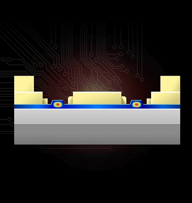
Inside a hyperscale rack, a wall of GPUs is hungry. They want data faster than copper can carry it and cooler than the power bill allows. The answer arriving on those boards is a chip most people will never see - a sliver of thin-film lithium niobate that flips electrons into photons and back, at over a hundred billion times a second, on less than a volt. A lot of those chips trace back to one building on Massachusetts Avenue in Cambridge.
That building belongs to HyperLight. The company designs and makes photonic integrated circuits - optical chips - on a material the industry spent two decades admiring from a safe distance. Lithium niobate has gorgeous electro-optic properties and a reputation for being almost impossible to manufacture at scale. HyperLight decided the reputation was the opportunity.
Today it runs what it describes as the industry's first and only high-volume, qualified 6-inch TFLN manufacturing line, with an 8-inch pilot already humming. That is the part competitors find inconvenient. Plenty of labs can make a beautiful modulator once. Making thousands, reliably, with a datasheet you can build a product around - that is a different sport.
Every generation of AI wants more bandwidth between chips. The traditional way to move that data optically is the silicon-photonics modulator - useful, mature, and increasingly stretched. To push more bits, you crank the drive voltage and the power, and the heat, and the bill. At some point the curve stops being friendly.
Lithium niobate sidesteps the trade. Its electro-optic effect is fast and linear, which means you can modulate light at enormous bandwidth without the voltage penalty. Engineers have known this since the era of bulky telecom modulators. The catch was always the same: you could not shrink it onto a wafer and fabricate it like a CMOS chip. The crystal would not cooperate.
So the optics community admired the material the way one admires a difficult relative - warmly, from across the room. That is the tension HyperLight was built to resolve.
HyperLight spun out of Harvard in 2018, from the lab of Professor Marko Loncar at the School of Engineering and Applied Sciences. There, Mian Zhang and his colleagues worked out how to fabricate chip-scale electro-optic modulators in thin-film lithium niobate - the step that had stumped the field. The bet was simple to state and hard to do: take the lab recipe and make it a manufacturing process.
Pictured in spirit: the team that decided "notoriously difficult to work with" was a marketing line, not a verdict.
Early backing came from The Engine, the tough-tech incubator born out of MIT that funds science with long fuses. The pitch was not a quick app; it was a fabrication platform. That kind of company needs patient money and a cleanroom, in roughly equal measure.
HyperLight's core idea is the TFLN Chiplet platform: the superior optics of thin-film lithium niobate, fabricated with CMOS-like, scalable techniques. It is sold the way a foundry sells - process, design tools, multi-project wafer runs, packaging and testing - so customers can design around it instead of inventing it.
The modular ecosystem: qualified 6-inch production, 8-inch pilot, design kits and MPW runs.
Direct-detection transmitter chips for datacenter links - 200 Gbit/s per lane.
Coherent transmitter PICs reaching up to 1.6 Tbit/s per wavelength.
Sub-volt drive, >100 GHz bandwidth, ready to drop into a module.
Bespoke circuits and consulting for sensing, LiDAR, quantum and microwave photonics.
The headline spec is efficiency. HyperLight's PICs run at CMOS-level drive voltages with electro-optic bandwidth high enough to chase down to roughly 5 picojoules per bit at the wall plug. In a building where the power budget is the real ceiling, picojoules are the currency that matters.
One way to read HyperLight's pitch is to line up where TFLN sits against the modulator technologies it competes with. The bandwidth headroom is the part data center architects keep circling.
Approximate, illustrative figures drawn from public HyperLight and industry materials; real performance depends on device design. The point is direction, not a benchmark verdict.
Charts rarely settle an argument. This one mostly explains why so many transceiver roadmaps suddenly have a lithium niobate line item.
A platform is only as credible as the systems built on it. HyperLight's modulators keep turning up in other companies' record attempts. With Ciena, Keysight and McGill University, its TFLN device sat at the heart of a demonstration of a 3.2T link running eight lanes of 448G. At ECOC 2025, the same trio showed driverless 448G PAM4 transmission over 500 meters using a sub-volt direct-drive modulator - "driverless" meaning they skipped the power-hungry amplifier entirely.
The other proof point is industrial, not academic. In 2026 HyperLight and UMC - with the foundry's subsidiary Wavetek - announced a partnership to mass-produce the TFLN Chiplet platform on 6-inch and 8-inch wafers. A reference 1.6T-DR8 transceiver, assembled by TFC, was lined up to run live at OFC. Lab demos prove the physics. Foundry deals prove the business.
Led the $37M Series B; Peter Chung on the board.
Deep-tech fund backed by Temasek.
Returning Series B investor.
Seed-stage tough-tech backer.
Mass production on 6″ and 8″ wafers.
448G & 3.2T link demonstrations.
High-baud coherent transmission research.
Assembled the 1.6T-DR8 reference module.
HyperLight's stated belief is that integrated photonics is on a historic path to enable the next level of technology, and that thin-film lithium niobate is the material that unlocks it. The internal values it lists are unglamorous on purpose: integrity, innovation, collaboration, and pragmatic solutions. Pragmatic is the operative word for a company whose entire premise is doing the hard, boring manufacturing work that turns a great material into a shippable product.
The applications fan out from there: AI and data center interconnects first, then telecom optical networks, high-performance computing, and the longer-horizon work - LiDAR and sensing, microwave photonics, quantum. Each of those wants the same thing the data center wants: more bandwidth, less power, in a package you can actually buy.
Return to that hungry rack of GPUs. The thing that decides how big AI models can get is not only how fast the chips compute - it is how fast they can talk to each other without melting the building. Move that conversation onto light, at low voltage and high bandwidth, and the ceiling lifts.
That is the change HyperLight is selling, one wafer at a time. The crystal everyone admired from across the room is now coming off a production line in Cambridge, headed for the boards that train tomorrow's models. The hard part was never the physics. It was the manufacturing - and that is exactly the part they chose to build.
Footnote for skeptics: none of this is finished. Mass production is a verb, not a press release. But the line is running, and the orders are real.