laser-wafering
(2)
Andrei Iancu Is Teaching Factories to Cut Crystals With Light
The Halo Industries founder turned a Stanford materials problem into a semiconductor manufacturing company. His wager is practical: waste less of the crystal, learn faster on the factory floor, and let better power electronics follow.
Halo Industries, Inc.
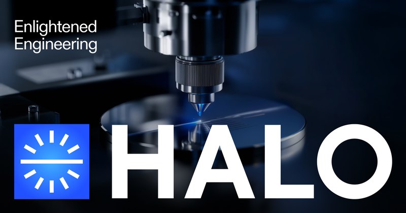
Halo Industries is a Santa Clara deep-tech company that uses lasers instead of diamond wire saws to slice silicon carbide crystal boules into wafers, the foundational substrate for high-voltage power electronics. Spun out of Stanford in 2014, its proprietary light-based process aims to eliminate kerf loss, cut defects, and slash water and energy use, giving more usable wafers from every expensive crystal. Backed by an $80M Series B, Halo is scaling SiC production for electric vehicles, grid infrastructure, renewables, and aerospace, and extending the same approach to silicon, sapphire, and diamond.