Before Robert Devlin learned to make a lens without a curve, he learned to make a voice appear out of a collection of parts. His grandfather, a former Navy radio operator, built shortwave radios in his basement. As a child, Devlin helped put them together. Components that looked unrelated became a machine that could hear someone far away. The surprise was both technical and human: another person, somewhere beyond the house, had entered the room.
Today, Devlin is co-founder and CEO of Metalenz, the company he helped start in 2016. Its optics use patterns of tiny structures to control light on a flat surface. They can be manufactured in semiconductor foundries, the industrial setting more commonly associated with computer chips. The components have changed dramatically since those basement afternoons. His interest in coaxing useful information out of invisible signals has lasted.
There is a pleasing continuity here. The radio asked what an arrangement of parts could let a person hear. The metasurface asks what an arrangement of materials can let a device see. Between those questions sits a career that has required Devlin to learn as much about factories and collaboration as about light.
An education with a factory floor
Engineering was already close to home. Devlin remembers visiting the factory where his father worked at Flexitallic, a gasket manufacturer. His father worked his way into global sales management. For the younger Devlin, the machinery, the people operating it and the eventual overseas customers belonged to the same picture. A product involved a whole chain of people before it reached the person buying it.
At Drexel University, he studied electrical and computer engineering alongside materials science and engineering, earning his bachelor’s and master’s degrees in 2013. The combination took him from processing signals to the substances and structures that made the components possible. It was a useful pairing for someone interested in what a device could do, and in how to build it.
Drexel’s co-op program gave that education somewhere to land. One placement brought him into professor Steve May’s research group. He worked on open research questions and learned from graduate students around him. He later credited that experience with preparing him for doctoral study and helping him form Metalenz. A syllabus can introduce uncertainty. A research project leaves you responsible for it.
The curve disappears
Devlin went to Harvard for a doctorate in applied physics, working in Federico Capasso’s laboratory. The group had been developing metasurfaces, flat optical elements whose tiny patterns influence light. The proposition was easy to admire. Conventional lenses rely on curved surfaces; stacking them helps correct distortions but takes space. A patterned surface offered another way to organize the light.
Admiration, however, does not improve an inefficient device. Devlin’s work involved materials and nanofabrication, with the practical aim of getting more light to go where the design required. For visible-light devices, the team used titanium dioxide, a material that could avoid the absorption losses undermining earlier approaches. Carefully fabricated nanofins supplied the structure needed to shape the wavefront.
In 2016, Devlin was a co-author of the Science paper demonstrating high-resolution imaging with visible-wavelength metalenses. A related PNAS paper, on which he was first author, demonstrated efficient dielectric metasurfaces for red, green and blue wavelengths. These were collective achievements, built with collaborators including Mohammadreza Khorasaninejad, Wei Ting Chen, Jaewon Oh and Capasso. The material choice and the fabrication process gave an intriguing idea a more useful physical form.
Several elements can share the optical work.
Nanostructures can combine functions in one element.
A cover story meets a production line
The Science work appeared on the journal’s cover and was recognized among its ten breakthroughs of 2016. Industry interest followed. Phone manufacturers, investors and people in optics began calling. Devlin had been considering an academic career. The calls raised a more immediate question: could the research become something people actually used?
He co-founded Metalenz that year with Capasso and Bart Riley. The company obtained an exclusive license to the foundational Harvard metasurface intellectual property. Devlin completed his doctorate in 2017. The transition put a different set of requirements around the same physics. A company needed a product that fitted a customer’s design and could survive the customer’s manufacturing expectations.
Three-dimensional sensing offered an opening. Its optical assemblies were complex, and reducing the number of components could make a practical difference. The expansion of phone-based face authentication also helped the timing. Devlin has recalled the arrival of Apple’s Face ID as a useful surprise: an emerging application gave the young company a market to investigate.
Metalenz adopted a fabless model, concentrating on designs while working with manufacturing partners. STMicroelectronics brought both semiconductor facilities and experience supplying sensing modules. The relationship joined a new optical approach to an existing route into products. In June 2022, Metalenz technology made its commercial debut in ST’s time-of-flight sensing systems.
“It’s really about having confidence that it’s going to last, that it’s going to be reliable.”
Robert Devlin, 2022
Reliability has fewer admirers than a striking research image, but it gets invited into more purchasing meetings. A manufacturer wants to know that the next device will behave like the last one, and that the process will keep doing so. For Devlin, proving that became part of the invention’s journey.
Ten thousand reasons to believe
The foundry produced an object that gave the change in scale a visible form: a 300-millimeter wafer holding 10,000 optical devices. Devlin has described receiving the first such wafers as a memorable moment. A single disc contained more devices than the lab had made through years of doctoral work. The promise of semiconductor production had acquired something you could hold.
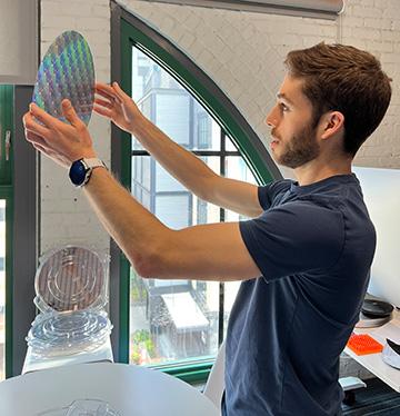
devices on a single
300 mm wafer
Reaching that point involved an awkward negotiation. Prospective customers wanted evidence of mass production. Prospective production partners wanted evidence of customers. Each request was sensible in isolation. Together, they could leave a startup politely waiting outside two doors. Getting both sides comfortable enough to proceed required confidence in the people as well as in the technology.
In October 2022, Metalenz announced a $30 million Series B. In June 2023, it announced a direct manufacturing supply chain with UMC for the open market. The company was building options beyond its initial licensing relationship, and the work expanded beyond optical designs into systems, software and algorithms.
By July 2025, ST said it had shipped well over 140 million metasurface optics and FlightSense modules using Metalenz intellectual property since 2022. The partners signed a broader licensing agreement. That count belongs to the commercial technology and its partner’s shipments; it gives a concrete measure of the distance traveled from the Harvard prototypes.
- 2016Research breakthrough;
Metalenz founded - 2022Commercial debut
with ST - 2023Direct supply chain
with UMC - 2025Expanded
ST license
The experiment gets more people
Devlin’s account of running a company makes space for the people required to move a design into a consumer device. The number of specialties involved has surprised him. A physicist can understand the optical principle and still need colleagues who understand production, supply chains, software and the customer’s constraints. The research grows more practical by becoming less solitary.
He has described wanting colleagues who can discuss unfamiliar ideas and accept being wrong. That preference has a direct engineering use: an unresolved problem should be allowed to challenge the person proposing the answer. His public praise of marketing colleague and artist Carly Glovinski points to a similar appreciation of varied experience. Different backgrounds can contribute to the same product without becoming interchangeable.
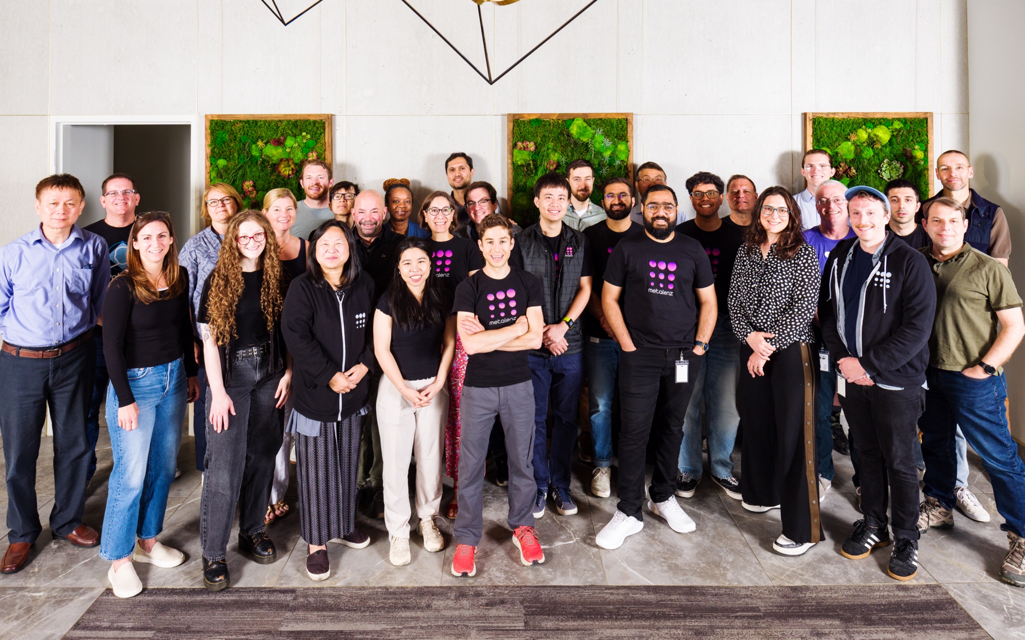
In 2025, Optica selected Devlin for the Kevin P. Thompson Optical Design Innovator Award. The recognition covered foundational metasurface design, commercialization and the development of consumer polarization sensing. It joined the research and the business in a single citation. His career had come to include the experimental result and the work of getting that result out of the laboratory.
What else is hiding in the light?
Making an optical assembly smaller was an initial use of Metalenz’s technology. Polarization offers another direction. Light has an orientation of oscillation as well as intensity and color. That polarization information can provide clues about surfaces and materials. A device designed to capture it can receive information a conventional imaging system leaves unused.
Metalenz developed Polar ID around that idea, combining polarization-sensitive optics with algorithms for face authentication. In November 2025, the company and UMC announced readiness for high-volume manufacturing. UMC’s process brings a metasurface layer together with an image sensor using wafer-on-wafer bonding. The announcement described manufacturing capability and a demonstrated reference platform, the foundations for pursuing wider adoption.
February 2026 brought Polar 3D, an announced extension of the platform into single-image capture of facial shape and reflections. The proposed uses include portraits whose lighting can be adjusted and avatars that preserve surface detail. The company’s approach separates information about reflection from the lighting in the original image. An awkwardly placed sun becomes a technical problem with an unusually relatable brief.
In May, Metalenz announced Polar ID Under Display, with a demonstration operating beneath a powered OLED smartphone screen. The appeal is easy to picture: authentication hardware could occupy less visible space on the front of a phone. Devlin described the relationship between the underlying device and that everyday result: “It starts at the metasurface hardware and flows to user experience.”
The next connection
Devlin’s ambitions have also included helping science and engineering students turn research into companies and products. In his Drexel alumni profile, he hoped to offer advice and perspective to people considering that route. His own experience gives him several useful places to begin: the material, the manufacturing process, the customer and the colleagues who know something you do not.
The childhood radio remains a good place to end. It offered a small, immediate demonstration that understanding components could connect you to another person. Devlin’s current work makes a similar wager at a different scale. Arrange the structures carefully enough, make them reliably enough, and a device can receive more of the world. Then comes the absorbing question of what people will do with it.
Keep following the signal
Conversations, research and recent developments.
- Metalenz’s website Products and company updates
- Robert Devlin on LinkedIn His public professional profile
- Watch: Devlin and Federico Capasso discuss metasurface optics Optica interview, YouTube
- Watch: Devlin on TechFirst John Koetsier’s 2021 conversation, YouTube
- Watch: Devlin on the 632nm podcast Manufacturing and polarization, 2026
- Read the 2023 entrepreneur interview Optics & Photonics News
- From Capasso’s lab to consumer devices Harvard’s 2025 account
- Polar 3D announcement February 2026
- Polar ID Under Display announcement May 2026