Patrick
Bowen.
He runs an Austin chip company that makes matrix multiplications happen by shining infrared light through a piece of engineered glass.
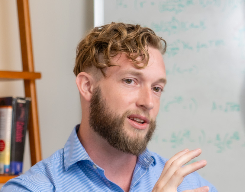
PATRICK BOWEN, CO-FOUNDER AND CEO, NEUROPHOS. He talks about photons the way most people talk about weather - casually, and with the faint suggestion that everyone else has been getting it wrong for a while.
The startup that wants AI compute to run at the speed of light.
Neurophos is a 55-person semiconductor startup in Austin, Texas, and its pitch is roughly this: the transistor, as currently practiced, has run out of interesting things to say to the AI industry. So Patrick Bowen and his co-founders are building a chip that skips the transistor entirely and does its arithmetic in light. In January 2026 they closed a $110 million Series A led by Gates Frontier, with Microsoft's M12 venture arm, Aramco Ventures, Bosch Ventures, Carbon Direct Capital, Tectonic Ventures and Space Capital along for the ride. Total funding is now about $118 million. There is no product yet. There is silicon, from May of 2025, which appears to work.
The idea is not new. Optical computing was fashionable in the 1980s, briefly, before it turned out that the modulators - the little devices that turn electrical signals into light - were too big, too slow, and too power-hungry to compete with the transistor. Bowen's argument is that metamaterials fix this. A metamaterial is a surface patterned at scales smaller than the wavelength of light, engineered to bend and manipulate photons in ways that ordinary glass cannot. His PhD advisor, David R. Smith at Duke, is the physicist who first demonstrated a negative-index metamaterial - the piece of physics that made the term "invisibility cloak" briefly plausible in newspapers. Bowen spent his graduate years in that lab, then a decade after it running Metacept, a metamaterials consulting firm he co-founded with Smith. Neurophos is what happened when he decided the best commercial application of two decades of metasurface work was AI chips.
The bet is scale. Neurophos's optical modulators, according to public statements from Bowen, are about 8,000 times smaller than the Mach-Zehnder interferometers you would get from a standard silicon photonics fab. The company claims a photonic tensor core on a single chip that is 1,000 by 1,000 processing elements - a million multiply-accumulate operations in a grid, all firing at roughly 56 gigahertz - and that this arrangement, called the "folded Goodman engine" in their marketing, can deliver 470 petaFLOPS of low-precision inference on a 1 to 2 kilowatt power envelope. The first chip is codenamed Tulkas T100. Tulkas, in Tolkien's cosmology, is the strongest and swiftest of the Valar; he laughs in battle. Production is scheduled for mid-2028.
Bowen is careful, in interviews, not to sell speed as such. His framing is about the ratio - compute per watt - because he understands that the constraint on hyperscale AI is no longer wafer, it's substation. "If you have a server that burns say 6 kilowatts," he told Semiwiki, "and you want to go 100 times faster but do nothing about the fundamental energy efficiency, then that 6 kilowatt server suddenly becomes a 600 kilowatt server." This is the kind of arithmetic that keeps data center operators awake, and it is the exact sentence a fund like Gates Frontier is presumed to want to hear. Their entire thesis is climate-adjacent bets on infrastructure that would otherwise become uneconomic.
There is a version of the Neurophos story that reads as a bet on a single person. The company spun out of an established physics lineage, from a well-known Duke lab, staffed by people who have been building metasurfaces since before AI became the reason anyone cared about them. Bowen was educated at ETH Zurich - a master's in micro-nano systems - and returned to the United States for his PhD, publishing on optical metamaterials and computational photonics. Somewhere in there he did a stint at Kymeta, the metamaterials-based antenna company backed by Bill Gates. Then Metacept. Then Neurophos. It is one of the more legible founder paths in the AI hardware business, which is otherwise crowded with GPU refugees and reformed cryptocurrency people.
The technical claim to watch is manufacturability. "We got our first silicon back in May," Bowen told The Register in January, "demonstrating that we could do that with a standard CMOS process." Standard CMOS is the phrase that unlocks the industry. It means you can make the chip in the same fabs that make everything else, which means yield curves, which means the difference between a research demonstration and a product. Optical computing companies have historically stumbled at exactly this seam - the physics worked in a lab, and then the lab could not be extruded into a foundry. Neurophos is betting that metasurfaces are foundry-friendly in a way that older photonic elements were not. The first silicon suggests they might be right. The next silicon will tell.
Bowen has also been unusually direct about the shape of his market. "We're talking thousands of chips," he told an interviewer. "Not tens of thousands of chips." This is the sound of a founder who has looked at the customer list for exaflop-class AI inference and counted about a dozen names. The strategy is concentration, not distribution: land one hyperscaler, one workload - Neurophos is aiming at LLM prefill first, the compute-heavy portion of inference where the tensor core does its most obvious work - and let the sales cycle be long and specialized. It's a market shape that fits the company. Neurophos does not want to sell you a laptop chip.
What makes Bowen interesting, at least in interviews, is that he does not sound especially like a hardware CEO. He sounds like a physicist who runs a company because someone had to. He talks about optical transistors the way an art critic talks about paintings - "the equivalent of the optical transistor that you get from Silicon Photonics factories today is massive, it's like 2 millimeters long" - as if the size of the thing were itself a moral failing. He references the 1980s optical computing effort not as a cautionary tale but as an unfinished project. His stated corporate purpose is to bring "the computational power of the human brain to artificial intelligence." Whether that is achievable at 56 gigahertz through a millimeter of engineered glass is a question a lot of very sophisticated investors have just spent $110 million trying to answer.
Neurophos, by ratio.
GPUs are not the answer to the future of AI workloads.— Patrick Bowen, Semiwiki interview
One chip, rendered as specs.
Neurophos Optical Processing Unit
Source: Bowen interviews with The Register, Semiwiki, Jon Peddie Research (2026)
Bowen, on photons.
We exist to bring the computational power of the human brain to artificial intelligence.Semiwiki
The equivalent of the optical transistor that you get from Silicon Photonics factories today is massive. It's like 2 millimeters long.The Register
We got our first silicon back in May demonstrating that we could do that with a standard CMOS process.The Register, Jan 2026
Just as GPUs were better than CPUs for neural networks, there could be architectures that are better than GPUs by orders of magnitude.Semiwiki
On chip, there is a single photonic tensor core that is 1,000 by 1,000 processing elements in size.The Register
We're talking thousands of chips. Not tens of thousands of chips.The Register
The path, briefly.
Small things, worth knowing.
His PhD advisor at Duke, David R. Smith, ran the first experimental demonstration of a negative-index metamaterial - the physics behind every "invisibility cloak" headline you have ever seen.
The first Neurophos chip is codenamed Tulkas, after the Tolkien Valar known as the strongest and swiftest of the gods, who laughs in battle.
Before Neurophos, he spent roughly a decade doing metamaterials for other companies through Metacept - a consulting shop he co-founded with his own PhD advisor.
The Series A investor list is unusually diversified for a chip startup: Microsoft's M12, Aramco Ventures, Bosch Ventures, Space Capital, Carbon Direct, Tectonic Ventures - each with a different angle on the same bet.
He describes the internal architecture as a "folded Goodman engine," after Joseph Goodman, whose 1970s work on Fourier optics is the intellectual root of most modern optical computing.
Total addressable market, per Bowen: "thousands of chips, not tens of thousands." Concentration is the strategy.
A short FAQ.
Who is Patrick Bowen?
Co-founder and CEO of Neurophos, an Austin-based chip startup building optical AI accelerators around metamaterial-based photonic tensor cores. Duke PhD in EE, ETH Zurich master's in micro-nano systems.
What is Neurophos actually building?
An optical processing unit - a chip whose core arithmetic is done by shining light through a metasurface. The first product, Tulkas T100, targets 470 petaFLOPS of low-precision inference in a 1-2 kW envelope, aimed at LLM prefill.
How much has the company raised?
About $118 million total, capped by a $110M Series A in January 2026 led by Gates Frontier, with M12, Aramco, Bosch Ventures, Tectonic Ventures, Space Capital, and Carbon Direct Capital.
Why metamaterials?
Because the standard silicon-photonics modulator is roughly 2mm long - too big to fit meaningful compute on a chip. Metasurfaces let Neurophos pack sub-wavelength modulators into a dense array, which they claim is about 8,000× smaller.
When does the first chip ship?
Bowen has said production is targeted for mid-2028. First silicon returned in May 2025 and reportedly worked.